Facebook
 Google
 GitHub
 Linkedin
Analog Multipliers
Consider the multiplier in Figure 18-6. We have seen a similar circuit before, used as a phase detector for a PLL. While accuracy in that application was of minor importance, in a multiplier it is the main feature.
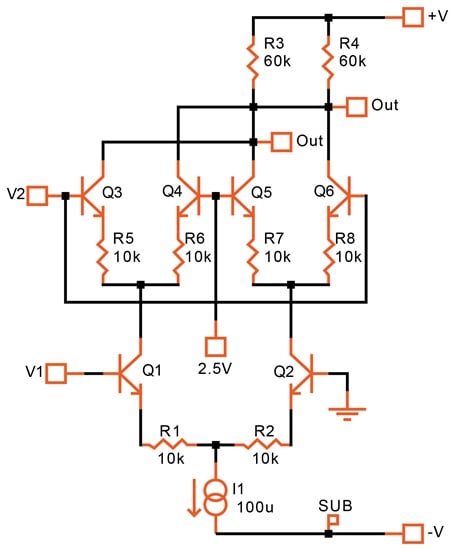
Figure 18-6. Simple four-quadrant multiplier.
The circuit requires a split power supply (in this example, ±5), so that at least one input (V1) can be at ground level. The second input (V2) is biased safely higher (2.5 V) to avoid saturating Q1 and Q2.
It is the insertion of resistors in the emitters of all six transistors that gives this multiplier its accuracy. Their values need to be large compared to the dynamic emitter resistance.
Such a circuit is called a four-quadrant multiplier because it produces an output for all four quadrants of a plot:
- Both inputs positive.
- V1 positive and V2 negative.
- Both inputs negative.
- V1 negative and V2 positive.
It must be noted that V2 is considered positive or negative with respect to its 2.5 V reference value.
In Figure 18-8, the range of the two input voltages is ±100 mV, resulting in a maximum output of ±10 mV. This limits the achievable accuracy, since VBE matching becomes as important a factor as matching of the resistors. A higher positive supply voltage is needed to allow input and output ranges of ±1 V.
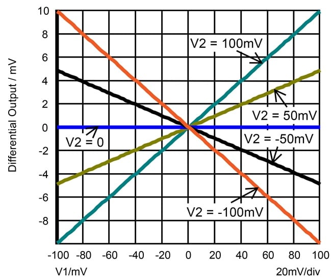
Figure 18-7. Behavior of the four-quadrant multiplier.
The error can be as high as ±5% untrimmed and ±1% trimmed. With a higher supply and trimmed thin-film resistors, ±0.3% is possible.
Figure 18-8 shows a four-quadrant multiplier with both inputs at ground level. This is accomplished by adding two transistors and biasing the upper quad (Q7 to Q10) with diode-connected transistors (Q5 and Q6, sitting at a DC potential set by R7). The ranges of the two inputs and the output are also now extended to ±1 V.
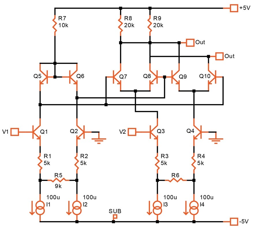
Figure 18-8. [click to enlarge] Four-quadrant multiplier with both input voltages at ground level.
Accuracy is unchanged for untrimmed operation. With trimmed thin-film resistors and additional temperature compensation, such a circuit can be brought to within 0.1%.
A CMOS Multiplier
Figure 18-9 shows the equivalent circuit in CMOS, designed for a 0.35 μ process.
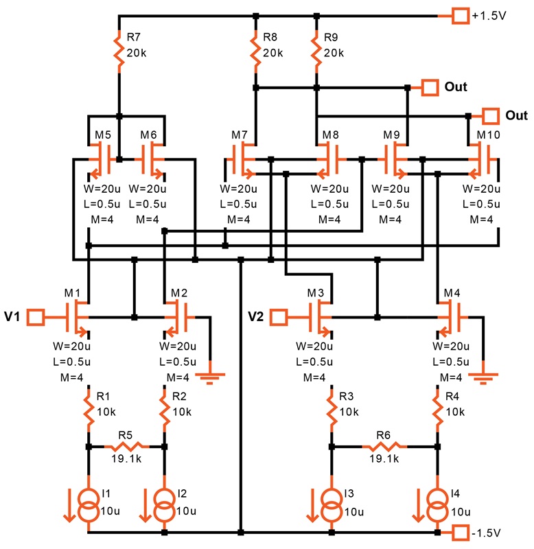
Figure 18-9. [click to enlarge] Four-quadrant CMOS multiplier.
Because of the lower supply voltages, the range of the input voltages is again limited to ±100 mV.
This circuit illustrates the performance limitations imposed by low supply voltages. With offset voltages generally being higher in CMOS and the maximum output range a mere ±10 mV, untrimmed accuracy is no better than about ±10%. You can, of course, change the resistor ratios so that the relationship between inputs and output is multiplied by a constant.