Facebook
 Google
 GitHub
 Linkedin
Digital Lab - 7-segment LED Display
Project Overview
The operating principle for this circuit (Figure 1) is to input a four-bit BCD (binary-coded decimal) value using the switches and energize the proper output lines to form the corresponding decimal digit on the 7-segment light-emitting diode (LED) display.
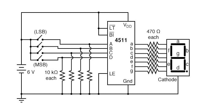
Figure 1. Schematic diagram of the 7-segment LED display circuit.
Parts and Materials
- 4511 BCD-to-7seg latch/decoder/driver
- Common-cathode 7-segment LED display
- Eight-position DIP switch
- Four 10 kΩ resistors
- Seven 470 Ω resistors
- One 6 V battery
Caution! The 4511 IC is a complementary metal-oxide semiconductor (CMOS) and, therefore, sensitive to static electricity!
Learning Objectives
- How to use the 4511 7-segment decoder/display driver IC
- Gain familiarity with the BCD code
- How to use 7-segment LED assemblies to create decimal digit displays
- How to identify and use both active-low and active-high logic inputs
Instructions
This experiment is more of an introduction to the 4511 decoder/display driver IC than it is a lesson in how to build a digital function from lower-level components. Since 7-segment displays are common components of digital devices, it is good to be familiar with the driving circuits behind them, and the 4511 is a good example of a typical driver IC.
Step 1: Connect the four switches to their pulldown resistors and the ABCD inputs of the 4511 IC, as illustrated on the left side of Figures 1 and 2.

Figure 2. Breadboard implementation of the 7-segment LED display circuit.
The BCD inputs are designated A, B, C, and D in order from least significant to most significant. The truth table for mapping these BCD inputs to the seven segment outputs is provided in Table 1.
Table 1. A truth table for 4511 IC BCD to 7-segment display driver
| BCD Inputs | 7-Segment Outputs | LED Display | |||||||||
|---|---|---|---|---|---|---|---|---|---|---|---|
| D | C | B | A | a | b | c | d | e | f | g | Digits |
| 0 | 0 | 0 | 0 | 1 | 1 | 1 | 1 | 1 | 1 | 0 | 0 |
| 0 | 0 | 0 | 1 | 0 | 1 | 1 | 0 | 0 | 0 | 0 | 1 |
| 0 | 0 | 1 | 0 | 1 | 1 | 0 | 1 | 1 | 0 | 1 | 2 |
| 0 | 0 | 1 | 1 | 1 | 1 | 1 | 1 | 0 | 0 | 1 | 3 |
| 0 | 1 | 0 | 0 | 0 | 1 | 1 | 0 | 0 | 1 | 1 | 4 |
| 0 | 1 | 0 | 1 | 1 | 0 | 1 | 1 | 0 | 1 | 1 | 5 |
| 0 | 1 | 1 | 0 | 0 | 0 | 1 | 1 | 1 | 1 | 1 | 6 |
| 0 | 1 | 1 | 1 | 1 | 1 | 1 | 0 | 0 | 0 | 0 | 7 |
| 1 | 0 | 0 | 0 | 1 | 1 | 1 | 1 | 1 | 1 | 1 | 8 |
| 1 | 0 | 0 | 1 | 1 | 1 | 1 | 0 | 0 | 1 | 1 | 9 |
Step 2: Connect the seven outputs from the 4511 IC to the corresponding inputs on the 7-segment display. Outputs are labeled a, b, c, d, e, f, and g, with each letter corresponding to a standardized segment designation for 7-segment displays. Of course, since each LED segment requires its own dropping resistor, we must use seven 470 Ω resistors placed in series between the 4511’s output terminals and the corresponding terminals of the display unit.
Step 3: All LEDs inside the display unit are made common to each other on one side, either cathode or anode. The 4511 display driver IC requires a common-cathode 7-segment display unit, which is what is used here. So, we must connect the cathode connection to the ground.
Step 4: Complete the remaining connections, illustrated in Figure 1, including power and ground.
Step 5: After building the circuit and applying power, operate the four switches in a binary counting sequence (0000 to 1001), noting the 7-segment display. A 0000 input should result in a decimal 0 display, a 0001 input should result in a decimal 1 display, and so on through 1001 (decimal 9).
Step 6: Test to see what happens for the binary numbers 1010 (10) through 1111 (15). Read the datasheet on the 4511 IC and see what the manufacturer specifies for operation above an input value of 9.
In the BCD code, there is no real meaning for 1010, 1011, 1100, 1101, 1110, or 1111. These are binary values beyond the range of a single decimal digit and so have no function in a BCD system. The 4511 IC is built to recognize this and output (or not output!) accordingly.
Step 7: Three inputs on the 4511 chip have been permanently connected to either Vdd or ground. These input pins are Lamp Test, Blanking Input, and Latch Enable. To learn what these inputs do, remove the short jumpers connecting them to either power supply rail (one at a time), and replace the short jumper with a longer one that can reach the other power supply rail.
For example, remove the short jumper connecting the Latch Enable input (pin #5) to the ground, and replace it with a long jumper wire that can reach all the way to the Vdd power supply rail. Experiment with making this input high (1) and low(0), observing the results on the 7-segment display as you alter the BCD code with the four input switches.
After you’ve learned what the input’s function is, connect it to the power supply rail enabling normal operation, and proceed to experiment with the next input (either Lamp Test or Blanking Input).
Once again, the manufacturer’s datasheet will inform the purpose of each of these three inputs. Also, note that the Lamp Test (LT) and Blanking Input (BI) input labels are written with boolean complementation bars over the abbreviations. Bar symbols designate these inputs as active-low, meaning that you must make each one low (0) in order to invoke its particular function.
Making an active-low input high (1) places that particular input into a passive state where its function will not be invoked. Conversely, the Latch Enable (LE) input has no complementation bar written over its abbreviation, and correspondingly it is shown connected to ground low (0) in the schematic of Figure 1 so as to not invoke that function.
The Latch Enable input is an active-high input, which means it must be made high (1) (connected to Vdd) in order to invoke its function.
Related Content
Learn more about the fundamentals behind this project in the resources below.
Textbook:
Resistor Guide:
Worksheets: