 Facebook
 Google
 GitHub
 Linkedin
Digital Lab - S-R Latch With Enable Input using NAND Gates
Project Overview
In this next project in the digital series, you will build and test the circuit shown in Figure 1.
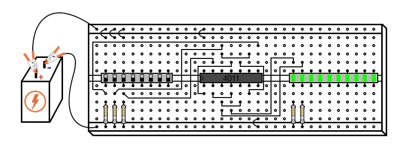
Figure 1. S-R enabled latch with switch inputs and LED outputs.
This circuit has three switch inputs at the left, a quad 2-input NAND gate IC in the middle, and output light-emitting diode (LED) status indicators at the right. It implements an S-R latch with a third, ENABLE, input added to the two inputs, SET and RESET, of the basic S-R latch.
Parts and Materials
- 4011 quad NAND gate
- Eight-position dual inline package (DIP) switch
- Ten-segment bar graph LED
- One 6 V battery
- Three 10 kΩ resistors
- Two 470 Ω resistors
Caution! The 4011 IC is a complementary metal-oxide semiconductor (CMOS) and, therefore, sensitive to static electricity!
Learning Objectives
- Principle and function of a latch circuit with ENABLE
- Digital circuit construction and testing
Instructions
Step 1: Review the pinout diagram in the datasheet for your 4011 CMOS quad NAND gate IC. It will be similar to Figure 1, but some of the pins may be different. Therefore, you may need to change the connections in the breadboard illustrations to match the pinout of your IC.
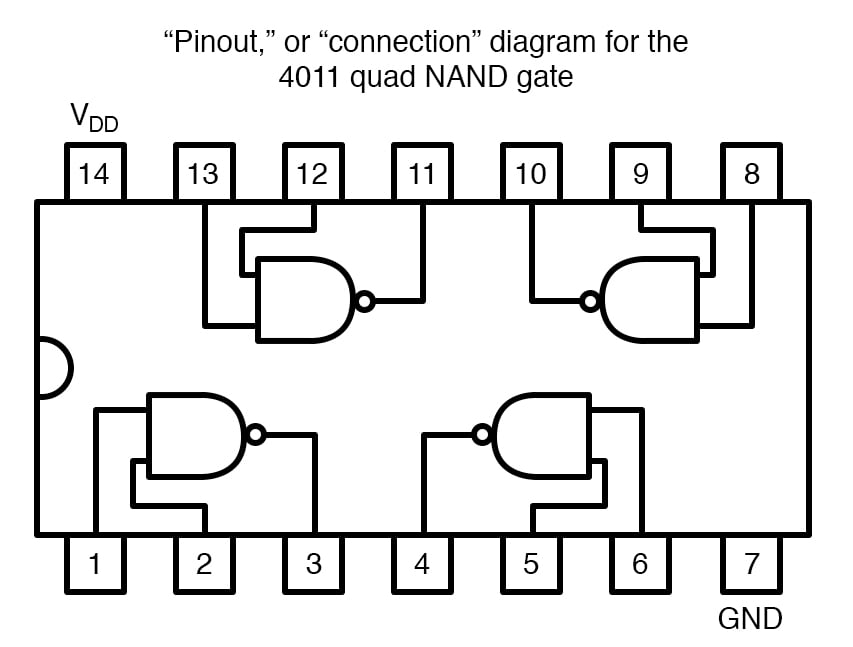
Figure 2. Typical pinout diagram for a 4011 CMOS quad 2-input NAND gate IC.
Step 2: Make the three switch connections to the 10 kΩ pull-down resistors at the left side of the circuit schematic of Figure 3 and the left side of the breadboard illustration of Figure 1.
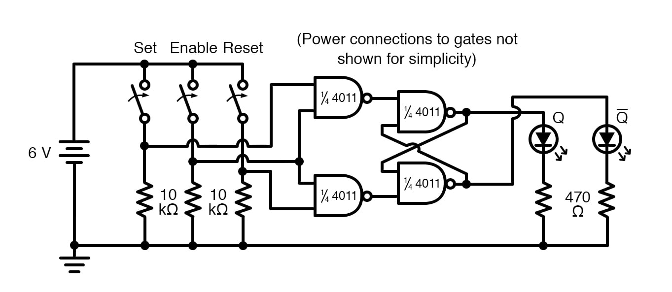
Figure 3. Schematic diagram of an S-R latch built using NOR gates.
Step 3: Wire up the four NAND gates, as illustrated in Figure 3. Although this circuit uses NAND gates instead of NOR gates, its behavior is identical to that of the NOR gate S-R latch.
Step 4: Finish the circuit by connecting the outputs of the two rightmost NAND gates to LEDs. Add 470 Ω resistors in series with the LEDs to limit the currents. If we assign the left switch as the SET input and the right switch as the RESET input, the left LED will be the Q output and the right LED the \[\overline{Q} \] output.
$$ \overline{Q} = \neg Q = ~!Q $$
Step 5: Test all of the input combinations of SET, RESET, and ENABLE. In a basic S-R latch, a high (1) SET input drives Q high (1), and a high (1) RESET input drives Q low (0). In this circuit, we must consider the presence of a third input, ENABLE. As its name suggests, the purpose of the ENABLE input is to enable or disable the SET and RESET inputs from having an effect on the circuit’s output status.
The truth table for the S-R latch with enable is provided in Figure 4.
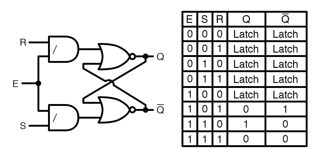
Figure 4. AND-NOR gate implementation (left) and truth table for the S-R latch with enable (right).
When the ENABLE input is high (1), the circuit acts just like the NOR gate S-R latch. When the ENABLE input is low (0), the SET and RESET inputs are disabled and have no effect whatsoever on the outputs, leaving the circuit in its latched state. Test all of the possible inputs yourself to verify that you have connected your circuit correctly and that the circuit does indeed provide this functionality.
This kind of latch circuit (also called a gated S-R latch) may be constructed from two NOR gates and two AND gates, as illustrated in Figure 4, but the NAND gate design is easier to build since it makes use of all four gates in a single integrated circuit.
Related Content
Learn more about the fundamentals behind this project in the resources below.
Textbook:
Resistor Guide:
Worksheets:
- Basic Logic Gates Worksheet
- Basic Logic Gate Troubleshooting Worksheet
- Latch Circuits Worksheet
- CMOS Logic Gates Worksheet


