 Facebook
 Google
 GitHub
 Linkedin
Digital Lab - S-R Flip-flop Using NAND Gates
Project Overview
In this project, you will build and test a NAND gate implementation of an S-R flip-flop with switch inputs and light-emitting diode (LED) output indicators, as shown in Figure 1.

Figure 1. S-R flip-flop with switch inputs and LED outputs.
As you will see, a flip-flop is edge-triggered, while a latch is level-sensitive.
Parts and Materials
- 4011 quad 2-input NAND gate IC
- 4001 quad 2-input NOR gate IC
- Eight-position dual inline packaging (DIP) switch
- Two LEDs or a ten-segment bar graph LED
- 6 V battery
- Three 10 kΩ resistors
- Two 470 Ω resistors
Caution! The ICs are complementary metal-oxide semiconductors (CMOS) and, therefore, sensitive to static electricity!
The illustration of Figure 1 shows two individual LEDs being used for the output indicators. This is due to a lack of room on my breadboard to mount the switch assembly, two integrated circuits, and the bar graph. If you have room on your breadboard, feel free to use the bar graph LED as called for in the parts list and as shown in other latch circuit projects.
Learning Objectives
- The difference between a gated latch and a flip-flop
- How to build a pulse detector circuit
- Learn the effects of switch contact bounce on digital circuits
Instructions
Step 1: The only difference between a gated (or enabled) latch and a flip-flop is that a flip-flop is enabled only on the rising or falling edge of a clock signal rather than for the entire duration of a high enable signal. So, begin by building the S-R latch with enable that is everything in the schematic diagram of Figure 2 except for the four NOR gates at the bottom of the figure.
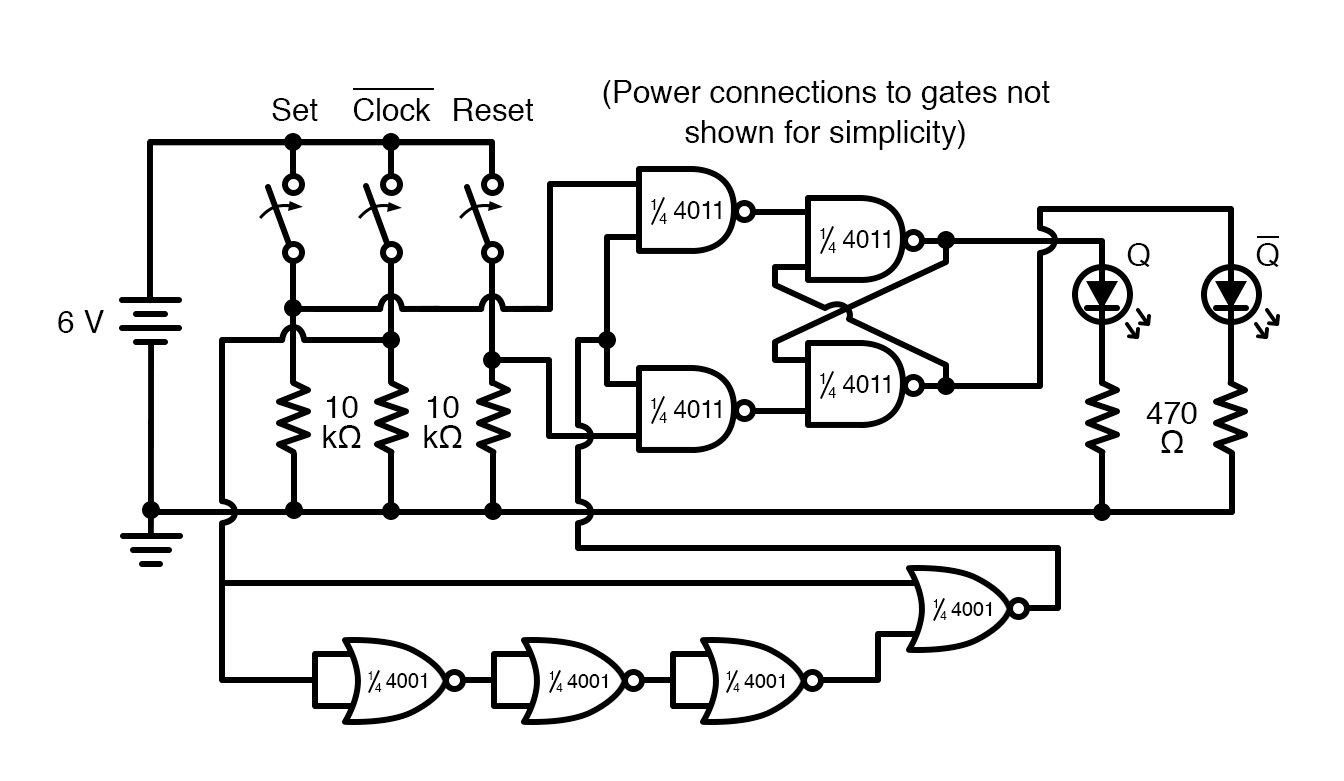
Figure 2. Schematic diagram of the S-R flip-flop with switch inputs and LED output indicators.
Step-by-step instructions for the S-R latch with enable are available here.
Step 2: Next, we will convert the enabled latch into a flip-flop by adding a pulse detector (or one-shot) circuit that generates a short pulse, as illustrated in Figure 3.

Figure 3. Gate logic and timing diagram for a simple pulse detector circuit.
The single NOR gate and three inverter gates create this effect by exploiting the propagation delay time of multiple cascaded gates.
In this experiment, I use three NOR gates with paralleled inputs to create three inverters, thus using all four NOR gates of a 4001 integrated circuit, as shown in Figure 4.

Figure 4. Implementation of a pulse detector circuit using four NOR gates.
Normally, when using a NOR gate as an inverter, one input would be grounded while the other acts as the inverter input to minimize input capacitance and increase speed. Here, however, the slow response is desired, so I parallel the NOR inputs to make inverters rather than use the more conventional method.
Please note that this particular pulse detector circuit produces a high (1) output pulse at every falling edge of the clock (input) signal. This means that the flip-flop circuit should be responsive to the SET and RESET input states only when the middle switch is moved from ON to OFF, not from OFF to ON.
Step 3: Connect the pulse detector from the second input switch, which will be our clock input, to the ENABLE input of the S-R Latch.
Step 4: First, test the circuit by setting the clock switch high (1) and cycling through different combinations of the SET and RESET inputs. The output should not change since there is no clock edge signal.
Step 5: Now, repeat the possible SET and RESET input combinations, and switch the clock switch from high (1) to low (0) after each change. The falling edge of the clock pulse generates a brief high (1) ENABLE pulse, as illustrated in Figure 3. This brief ENABLE period should be sufficient to allow your flip-flop to change states as a function of the SET and RESET inputs.
Step 6: Repeat Step 5, but by switching the clock switch from low (0) to (high). Ideally, nothing would happen. However, when you test this circuit, you may discover that the outputs respond to SET and RESET input signals during both transitions of the clock input, not just when it is switched from a high (1) state to a low (0) state. The reason for this is contact bounce, the effect of a mechanical switch rapidly making and breaking when its contacts are first closed due to the elastic collision of the metal contact pads.
Instead of the clock switch producing a single, clean low-to-high signal transition when closed, there will most likely be several low-high-low cycles as the contact pads bounce upon off-to-on actuation. The first high-to-low transition caused by bouncing will trigger the pulse detector circuit, enabling the S-R latch for that moment in time, making it responsive to the SET and RESET inputs.
Ideally, of course, switches are perfect and bounce-free. In the real world, though, contact bounce is a very common problem for digital gate circuits operated by switch inputs and must be understood well if it is to be overcome.
Related Content
Learn more about the fundamentals behind this project in the resources below.
Textbook:
Resistor Guide:
Worksheets:
- Flip-Flop Circuits Worksheet
- Basic Logic Gates Worksheet
- Basic Logic Gate Troubleshooting Worksheet
- Latch Circuits Worksheet
- CMOS Logic Gates Worksheet


