Facebook
 Google
 GitHub
 Linkedin
Analog Integrated Circuits
Design Project: Pulse-Width Modulation (PWM) Signal Generator
6 questions By Tony R. Kuphaldt
-
Question 4 of 6
It is important to not make resistor R1 too small in value. Explain why, and what might happen if it were.
Reveal answerIn the 555’s discharge cycle, resistor R1 will drop (almost) the full power supply voltage when Rpot1 is set for minimum resistance. Not only could this overheat R1, but it could also damage the discharge transistor within the 555 timer.
Notes:In order to really understand why insufficient resistance at R1 would be a bad thing, students must understand the astable operating cycle of the 555 timer. This question provides a very practical context in which to explore and/or review it!
-
Question 5 of 6
For those of you who are used to working with regular opamps, the presence of resistor R4 may be a mystery. It is necessary because of a special limitation of the type LM339 comparator IC. Research and explain what this limitation is.
Reveal answerThe LM339 comparator is only able to sink current at its output. Therefore, R4 acts as a pullup resistor.
Follow-up question: is this (overall) circuit capable of sourcing current to a load? Explain why or why not.
Notes:This characteristic of the LM339 caused problems for me the first few times I tried to use it in my designs. Despite this limitation, though, the LM339 is very aptly suited for this application with its fast response and very wide power supply voltage limits.
-
Question 6 of 6
The following modification may be made to the circuit to provide it with additional output current capability:
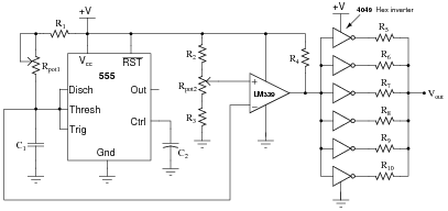
Here, six CMOS inverters (IC part number 4049) are ganged together in parallel to supply significantly more sourcing and sinking current capability than the LM339-with-pullup-resistor could on its own. Since CMOS logic gates are inherently on-or-off devices, they have no trouble handling the square wave output of the LM339.
Two questions here: first, why all the resistors at the outputs of the inverter gates? Why not just connect all the inverter outputs directly in parallel? Secondly, what value of resistor would you suggest at the output of each gate (R5 through R10)?
Reveal answerThe resistors prevent the (unlikely) occurrence of a short-circuit between two or more inverter gates, if one gate happens to fail high or low, or if some gates are significantly slower than others (and thus will “fight” with the faster gates during each transition).
Challenge question: adding inverter gates to the output of this circuit has an interesting effect on the duty cycle control. The potentiometer will now act backward from the way it was before (decreasing duty cycle when it formerly increased duty cycle, and visa-versa). Explain why.
Notes:This question may or may not be suitable for your students, depending on whether or not they have studied logic gates yet. If they have not yet studied digital circuits, it may be wise to skip this question!
Note that I did not answer the question of resistor sizes. Discuss this with your students, and let them determine how these resistors should be sized. Let them have access to datasheets for the 4049 inverter IC, and ask them what parameter(s) would be the most important in this decision.
If no one notices, point out how the power supply wires are drawn for the six-gate (hex) inverter. This is a common way to show power wiring for multiple gates (or opamps, or any other sort of IC where complex elements are duplicated).