 Facebook
 Google
 GitHub
 Linkedin
The Ripple Effects of Robert H. Dennard, Inventor of DRAM and Dennard Scaling
Dr. Robert Dennard passed away last month. He dedicated more than half a century of his professional life to microelectronics research, resulting in pivotal MOSFET scaling equations and DRAM.
Robert H Dennard, known with affection among his friends and colleagues as Bob, died on April 23, 2024, at age 91. He leaves behind an inspiring legacy and a rich body of work, including his invention of dynamic random-access memory (DRAM) in the late 1960s. That breakthrough paved the way for modern computer memory systems. We are re-publishing this article in tribute to Dr. Dennard and to his contribution to engineering and engineers. (Originally published on February 9, 2022.)
Smartphones are ubiquitous. Tablets are commonplace. Laptops continue to displace desktops. The miniaturization of sophisticated computational devices is a basic feature of our lives and has been for years.
As the age of vacuum tubes and room-sized computers fades deeper into the obscure recesses of our collective memory, we do well to consider the engineers whose diligence, brilliance, and ingenuity made the digital revolution possible. Robert Dennard was one of these engineers.
From Student to IBM Researcher
Robert H. Dennard was born in Terrell, Texas, in 1932. He attended Southern Methodist University in Dallas, earning a bachelor’s degree and a master’s degree in electrical engineering. He then continued with doctoral studies at the Carnegie Institute of Technology (now Carnegie Mellon University).
Dennard completed his PhD in 1958. That same year, he joined IBM as a research engineer and began investigating new logic and data-storage circuits.

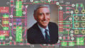
Robert H. Dennard. Image used courtesy of IBM
During those early days at IBM, he probably never imagined that fifty years later, he would be working for the same company and performing research in the same general field—using a personal computer made possible by the digital memory circuit that he invented!
The Single-transistor Memory Cell
In 1966, while exploring semiconductor-based alternatives to magnetic data-storage devices at IBM’s Thomas J. Watson Research Center, Dennard developed the circuit for which his name is now permanently engraved in the history of microelectronics and digital computing systems.
The essence of his accomplishment is this: his new architecture used one transistor (and one capacitor) to store one bit of data; the preceding architecture required six transistors.
SRAM vs. DRAM
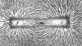
Digital computing systems need memory, i.e., circuitry that can “remember” (and reproduce) a given input state after that input state is no longer present. Basic logic gates (AND, OR, XOR, etc.), as well as standard feed-forward combinations of basic logic gates, cannot behave in this way: when an input signal changes, the output signal immediately responds.
However, logic gates can function as memory elements when they are interconnected in a feedback configuration. The diagram below depicts a rudimentary memory circuit, called a latch, consisting of two feedback-connected NOR gates.

The logic diagram for an SR latch.
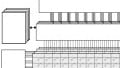
Research engineers at IBM were studying a six-transistor memory cell when Dennard first formulated the single-transistor approach. The six-transistor configuration is still useful; it is now known as “static” random-access memory (SRAM) because as long as power is supplied to the circuit, the stored bit value is stable.

A six-transistor circuit that can store one bit of data.
Though effective and conceptually straightforward, SRAM was an obstacle to high-density data storage. Dennard’s breakthrough was the realization that a logic voltage can be stored temporarily by an ordinary capacitor, and that this temporary storage can be prolonged indefinitely by periodically refreshing the capacitor.
This insight led Dennard to the invention of dynamic RAM (DRAM). In contrast to static RAM, dynamic RAM stores data via an inherently unstable mechanism. To function as memory for a computer system, DRAM cells require both constant application of power and continual refresh effectuated by a supplementary logic circuit.
As shown in the diagram below, the capacitor in a DRAM cell is charged or discharged through a field-effect transistor (FET) gated by one of the memory module’s read/write control signals.

Dennard’s DRAM architecture allows one bit of data to be stored by a smaller circuit comprising only one transistor and one capacitor.
When the FET is cut off, it presents a high impedance to the capacitor, which still experiences leakage discharge but nonetheless can maintain adequate voltage until the next refresh. When the FET is driven into conduction, the capacitor is connected through low impedance to the bit line, which either senses the capacitor’s voltage (for a read operation) or drives the capacitor’s voltage to the desired logic state (for a write operation).
This new RAM architecture resulted in dramatically higher memory densities and was therefore instrumental in the rapid advancement of digital computing systems. An article by John Markoff, posted on IBM’s THINK blog, says it well: Dennard’s invention “became the foundational technology for an industry that has reshaped human society.”
Moore’s Law and Dennard Scaling
Though remembered above all for his single-transistor memory cell, Robert Dennard has another claim to engineering fame: he was the principal developer of MOSFET scaling equations that became the theoretical basis for Moore’s law. This well-known “law” of microelectronics—formulated by Gordon Moore, co-founder of Intel—describes a trend pertaining to the steadily increasing density of transistors in integrated circuits.

MOSFET scaling relationships from Dennard’s seminal 1974 paper entitled “Design of Ion-Implanted MOSFET's with Very Small Physical Dimensions.” Image used courtesy of Auburn University
Moore’s law was essentially a rough prediction that became an observed reality. Dennard’s work, in contrast, led to specific mathematical relationships between MOSFET dimensions and fundamental electrical and manufacturing parameters. Published in 1974 and collectively known as Dennard scaling, these relationships became crucial guiding principles for the evolution of integrated-circuit technology.
“Attitude is Everything”
Dynamic RAM and MOSFET scaling are by no means an adequate summary of Dennard’s long and remarkably productive career as a research engineer. Holder of over 40 patents, author of numerous technical publications, recipient of the IEEE Edison Medal, the Benjamin Franklin Medal in Electrical Engineering, the IEEE Medal of Honor, et al.—Dr. Dennard brought talent, diligence, and creativity to his work and ended up creating an inflection point in the progression of modern technology.
Dennard posted the epigram “attitude is everything” in his bedroom, where he would see it every day. In his acceptance speech for the Kyoto Prize in Advanced Technology, he insisted that attitude “is the key to unleashing creativity. A great many have the intelligence, many have the preparation, some are at the right place at the right time, and only a few realize that they have the mission and ability to make a major difference in our world.”
Modern society is subject to an endless succession of new problems, and we are ever in need of new solutions. Robert Dennard’s career is an inspiration for all those who seek a brighter future for the human family, and his words should remind us that our attitude—rather than intelligence, education, or material resources—may prove to be the greatest obstacle to a life of enriching and enduring accomplishments.


It is sad to hear of the passing of Dr Robert Dennard. In my many years working at IBM’s Thomas J. Watson Research Center, I had the good fortune to work directly with Bob a number of times. I must say in such a community of really great minds, he certainly stood out. Besides being so incredibly creative, he was uncannily quick to grasp new ideas and concepts, and run with them even more than those who had far more familiarity with them. Bob was truly a genius, and his death is a great loss. However, I must also mention that in addition to his scientific achievements, Bob was a kind, soft spoken gentleman, without any of the “attitude” that often accompanies people of accomplishment.