Facebook
 Google
 GitHub
 Linkedin
Understanding Charge Amplifier Errors—Time Constant and Drift
Learn about charge amplifier limitations at low frequencies, the effects of time constants, and how the drift phenomenon can also introduce errors in low-frequency measurements.
In a previous article, we discussed that the time constant of a charge amplifier can limit the accuracy when measuring static signals. In this article, we’ll continue our discussion and examine more closely the limitations of using a charge amplifier at low frequencies. In doing so, we’ll see that, in addition to the time constant, the drift phenomenon can also introduce an error in our low-frequency measurements.
Charge Amplifiers With Adjustable Time Constants
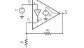
As depicted in Figure 1, the feedback path of some charge amplifiers incorporates both a switchable resistor as well as a reset/measure switch. This configuration enables the adjustment of the amplifier’s time constant depending on the low-frequency content of the input signal.
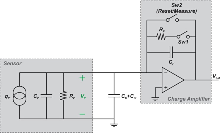
Figure 1. An example charge amplifier feedback path using a switchable resistor and reset/measure switch.
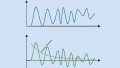
With the feedback resistor in place (i.e. SW1 closed and SW2 open), the limited time constant might be a source of error when measuring DC (or very low frequency) signals. As an example, consider applying the trapezoidal acceleration signal depicted in Figure 2a to the sensor. In this case, the flat parts of the output waveform can decay with time due to the short time constant of the system (Figure 2b).
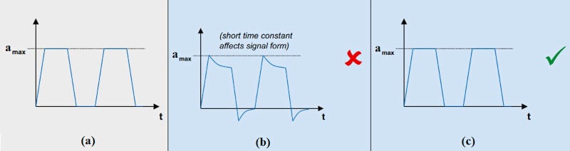
Figure 2. Examples of trapezoidal acceleration signal (a), how short time constant decays the output waveform (b), and accurate measure of the trapezoidal signal (c). Image (adapted) used courtesy of Kistler
To combat this problem, the time constant should be increased with respect to the input pulse width to limit the error. It can be shown, down below, that for a maximum error of 2%, the flat region of the input signal should not exceed 2% of the amplifier’s time constant.
$$\tau=R_{F}C_{F}$$
For example, if the input signal remains constant for 100 seconds, the time constant should be at least 5000 seconds to keep the error below 2%.
In fact, the discharge curve of an RC circuit can be considered relatively linear up to about 10% of the circuit time constant. Based on this point, we can determine the error percentage for a given time duration when dealing with static signals. For example, we can conclude that the sensor discharges by 1% in a time duration of 1% of $$\tau$$.
Thus, to have 1% accuracy in quasi-static measurement, we must take the reading of the output within a time window of 1% of the sensor time constant. Similar statements can be made up to about 10% of $$\tau$$.
Using the reset/measure mode of operation (SW1 open and SW2 is either on or off depending on being in the reset or measure phase of operation), we can maximize the time constant and more accurately measure the trapezoidal signal (Figure 2c). However, this can make the circuit more susceptible to drift.
Drift refers to a change in the output of the charge amplifier that occurs over a period of time and is not caused by a change in the physical parameter being measured (acceleration in our discussion). There are several different mechanisms that can lead to drift, which we'll investigate in the following sections.
Drift Cause One—Op-amp Input Bias Current
One source of the drift is the input bias current of the op-amp. Figure 3 illustrates the effect of the op-amp input bias current.
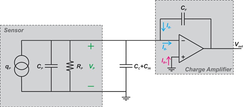
Figure 3. Diagram of a sensor and charge amplifier showing the op-amp input bias current.
In the above figure, IB- and IB+ denote the currents that flow into the input terminals of the op-amp. Note that the diagram shows the reset/measure mode of operation (RF is removed). Since the inverting input is at virtual ground, IB- can only flow through the feedback capacitor. This gradually charges CF and makes the output drift over time. Assume that IB-=10 fA and CF=1 nF. Also, suppose that CF is initially discharged.
With these values, the output voltage after 100 seconds can be found as:
$$V_{\,out} = \frac{1}{C_{F}}\int\limits_{t=0}^{100}I_{B-}dt = \frac{10fA\times(100-0)\,second}{1\,nF}=1\,\,mV$$
As you can see, after 100 s, the output drifts by 1 mV. This can cause issues especially when a small signal comparable with the error is being measured. Note that charge amplifiers that use a feedback resistor are more robust to the drift phenomenon. The impedance of CF is ideally infinite at DC. With RF in place, the dominant component of the feedback path at DC is a resistor. Since the feedback path is resistive rather than capacitive, the circuit cannot act as an integrator. In this case, IB- can cause only a DC shift between the output and the inverting input but it cannot ideally cause a drift.
Drift Cause Two—Op-amp Input Offset Voltage
Another mechanism that can cause drift is the input offset voltage of the op-amp. This is illustrated in Figure 4.
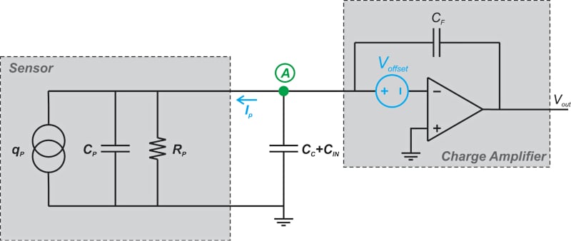
Figure 4. Diagram of a sensor and charge amplifier showing the op-amp input offset voltage.
Assuming that the op-amp has a high gain, it can be shown that the potential of node A is approximately equal to Voffset.
Therefore, the current flowing through the sensor insulation resistance can be found as:
$$I_{\,p} = \frac{V_{\,A}}{R_{p}} = \frac{V_{\,Offset}}{R_{p}}$$
This current is supplied through the feedback capacitor CF and can cause a drift just as the input bias current of the op-amp does. As an example, assume that:
- Voffset = 5 mV
- Rp = 10 TΩ
- CF = 1 nF
Assuming that CF is initially discharged, the output voltage after 100 seconds can be found as:
$$V_{\,out} = \frac{1}{C_{F}}\int\limits_{t=0}^{100}\frac{V_{\,Offset}}{R_{P}}dt=\frac{5\,mV\times(100-0)second}{10^{13}\Omega\times1\,nF} = 50 \,\mu V$$
This should be negligible in many applications; however, it should be noted that the sensor insulation resistance reduces significantly at higher temperatures. For example, at 400°C, the sensor insulation can drop to as low as 10 MΩ. In this case, a 5 mV offset can lead to a drift of 10 V just in 20 seconds and completely saturate the amplifier. Again, with RF in place, the DC current produced by the offset voltage cannot charge CF and the drift issue is ideally resolved.
Drift Cause Three—The Dielectric Memory Effect
The dielectric memory effect, or dielectric absorption, is a non-ideal effect that can produce an error voltage across a capacitor. As shown in Figure 5, assume that we charge a capacitor to a certain voltage and then discharge it over a short period of time (from t1 to t2).
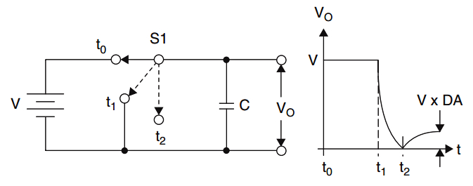
Figure 5. The residual open-circuit voltage after discharge/charge capacitor dielectric absorption. Image courtesy of Analog Devices' Linear Circuit Design Handbook
Next, we leave the capacitor disconnected. We ideally expect the open-circuit voltage of the capacitor to remain at zero volts. However, a residual voltage slowly builds up across the capacitor. For example, if the initial voltage of the capacitor was 2.5 V, the error voltage can be about 120 mV for a typical capacitor.
The dielectric memory effect is more noticeable when we discharge the capacitor quickly. The error voltage is proportional to the initial voltage of the capacitor as well as the properties of the capacitor dielectric. This effect can cause problems in the function of sensitive circuits such as sample and hold circuits, integrators, and voltage-to-frequency converters. In charge amplifiers, the dielectric memory effect in the feedback capacitor can produce a drift.
In addition to the effects discussed above, there are other drift mechanisms that can introduce errors in charge amplifiers. To learn about these drift mechanisms, please refer to the book “Piezoelectric Sensorics” by G. Gautschi.
What if the Drift Current Is Not Pure DC?
We discussed above that placing RF in parallel with the feedback capacitor can ideally resolve the drift issue because it creates an alternative path for the DC current produced by the drift mechanisms and doesn’t allow the drift current to charge the feedback capacitor. The question to be asked now is, what if the drift current is not a pure DC value and has some fluctuations?
For example, the input bias current of a FET (field-effect transistor) op-amp typically doubles with every 10°C rise in temperature. As a result, if our signal conditioning electronics experience large temperature variations, the drift-induced current might not be considered a pure DC value. In this case, we need to choose a relatively smaller RF to keep the feedback path still resistive at the frequency of the drift current. However, this remedy is achieved at the cost of a larger time constant error.
Figure 6 can help you better visualize the effect of temperature variations on the performance of charge amplifiers.
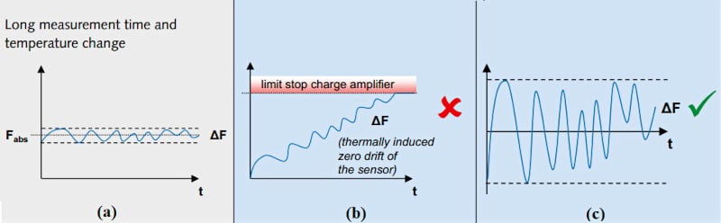
Figure 6. Visual examples of temperature variation effects on charge amplifier performance. Image used courtesy of Kistler
Figure 6a depicts the force acting on a piezoelectric sensing element, while Figure 6b shows the response of a charge amplifier that has a very large time constant and is susceptible to drift. Although the amplifier attempts to produce an output signal proportional to the applied force, it eventually saturates due to the thermally induced drift. However, an amplifier with a shorter time constant successfully amplifies the input signal.
Note that, in addition to reducing the time constant, there are several other complicated drift compensation techniques in the literature. For more information, you can refer to this research paper on drift compensation in charge amplifiers by Kos et al.
To see a complete list of my articles, please visit this page.
Related Content