Facebook
 Google
 GitHub
 Linkedin
Processing a Piezoelectric Accelerometer Output Using a Charge Amplifier
Learn about charge amplifiers which are used for charge output conversion of a piezoelectric sensor into a usable voltage signal.
In a previous article, we discussed the basics of piezoelectric accelerometers. In this article, we’ll look at charge amplifiers that are commonly used to convert the charge output of a piezoelectric sensor into a usable voltage signal.
Background on Piezoelectric Accelerometers
Using a piezoelectric element, a piezoelectric accelerometer produces a charge output proportional to the applied acceleration. A charge output is a difficult type of signal to measure because it can gradually diminish over time through leakage resistance.
Besides, the typical sensing elements used in piezoelectric accelerometers, these sensors produce a small amount of charge in the range of tens or hundreds of picocoulombs per newton. As a result, a signal conditioning circuitry is often required to successfully extract the acceleration information without any charge being dissipated. This requires amplification stages with large input impedance to prevent the produced charge from leaking off through the input impedance of the amplifier that is in parallel with the sensing element.
In fact, while the piezoelectric effect was discovered in 1880 by Pierre and Jacques Curie, it was of no practical use up until the 1950s due to a lack of amplifiers with sufficiently high input impedance. A charge amplifier is the technology of choice when processing the output of a piezoelectric sensor. Charge amplifiers convert the charge produced by the sensor to a usable voltage signal.
The articles “Understanding and Implementing Charge Amplifiers for Piezoelectric Sensor Systems” and “How to Design Charge Amplifiers for Piezoelectric Sensors” provide a good introduction to the basics of charge amplifiers.
Below, we’ll have a brief overview of the basic concepts along with some extra details.
Piezoelectric Sensor Equivalent Electrical Circuits
To get started, Figure 1 shows two equivalent electrical circuits that can be used to model a piezoelectric sensor.
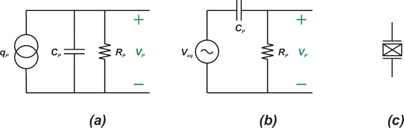
Figure 1. Two example circuit models (a) (b) for piezoelectric sensors along with their schematic symbol (c).
A piezoelectric sensing element consists of a dielectric material placed between two electrodes. When a mechanical force is applied, the sensor produces some charge. With that in mind, a piezoelectric accelerometer can be modeled as a capacitor that charges itself when subjected to acceleration. This usage leads to the circuit model in Figure 1(a). In this equivalent circuit, a charge source, qp, is placed in parallel with the capacitance of the sensor Cp. The resistor Rp models the insulation resistance of the sensor that creates a leakage path for the produced charge.
Figure 1(b), on the other hand, depicts another circuit model that uses a voltage source in series with the sensor capacitor to take the effect of the produced charge into account. The output voltage of an open-circuit piezoelectric sensing element is equal to the produced charge qp divided by the capacitance Cp. In Figure 1(b), Veq is incorporated to produce the open-circuit voltage of the sensor. Finally, Figure 1(c) shows the typical schematic symbol of a piezoelectric sensor.
Charge Amplifier Configuration—Finding the Output Voltage
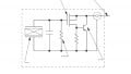
The basic configuration of a charge amplifier is shown in Figure 2.
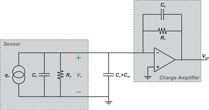
Figure 2. A schematic showing the configuration of a charge amplifier within a sensor.
In this figure, the capacitor CC + CIN models the cable capacitance plus the input capacitance of the charge amplifier. When the sensor is subjected to acceleration, the charge produced by the sensor, qp, appears across the capacitors Cp and CC + CIN.
The output voltage of the sensor attempts to change the potential of the inverting input of the op-amp. However, we know that due to the negative feedback mechanism and the high gain of the op-amp, the inverting input of the op-amp remains at virtual ground.
The op-amp actually transfers some electric charge to the inverting input to null the output voltage of the sensor and keep the inverting input at virtual ground. This charge is equal to the charge produced by the sensor and has the opposite polarity. The op-amp provides this charge through the feedback path, i.e. through the combination of RF and CF.
With an appropriately designed charge amplifier, RF is much larger than the impedance of CF in the frequency range of interest. Therefore, CF is the dominant element in the feedback path, and the charge the amplifier transfers to the inverting input is provided through the feedback capacitor. In other words, the charge amplifier compensates for the electric charge yielded by the sensor, qp, with an equal charge of opposite polarity in the feedback capacitor CF.
Thus, the output voltage, which is equal to the voltage across CF, can be found as:
$$V_{\, out} = -\frac{q_{p}}{C_{F}}$$
Main Advantages of Using a Charge Amplifier
With a charge amplifier, the voltage across the sensor is ideally zero. Therefore, no current can flow through any insulation resistance in parallel with the sensor such as the insulation resistance of the cable or the leakage resistance of the sensor Rp. Thus, the charge produced by the sensor is not dissipated. Besides, the output voltage is only a function of the feedback capacitor and hence, the sensor and cable capacitance cannot change the gain of the circuit.
Charge Amplifier Time Constant Parameter—Feedback Resistor
The feedback resistor RF provides a DC path for the inverting input of the amplifier and sets the DC voltage of this node. However, adding this resistor can limit the accuracy when measuring a DC (or very low-frequency) acceleration signal.
As we discussed above, the charge produced by the sensor is transferred to the feedback capacitor through the charge amplifier operation. This charge can gradually leak off through the feedback resistor, which is in parallel with CF.
In fact, the quasi-static behavior of the amplifier is determined by the time constant parameter:
$$\tau=R_{F}C_{F}$$
In the context of charge amplifiers, the quasi-static (or near static) behavior refers to the measurement of signals that remain constant for a relatively long time duration. For measuring very low-frequency signals, the time constant should be maximized.
To better understand the effect of the time constant parameter on our measurements, consider the waveforms shown in Figure 3.
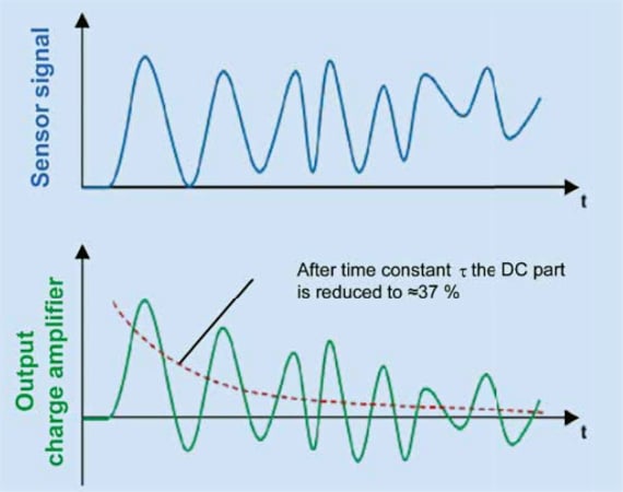
Figure 3. Output charge amplifier (bottom) and sensor signal (top) waveforms. Image used courtesy of Kistler.
In this figure, the top waveform shows the charge produced by the sensor, while the bottom waveform shows the output of the charge amplifier. In this example, it is assumed that the charge waveform has a fixed DC value along with some high-frequency components. The high-frequency components of the input appear at the output as expected. However, the DC value of the output, which is initially close to the DC value of the input, gradually approaches zero volts. This tendency is due to the fact that a static charge stored in CF leaks away through RF.
As you can see, after a time interval of one $$\tau$$, the DC value of the output is reduced to 37% of its initial value. With some types of charge amplifiers, it is possible to switch between different feedback resistor values to adjust the time constant parameter depending on the low-frequency content of the acceleration signal.
Charge Amplifiers With a Reset Switch
Alternatively, some charge amplifiers incorporate a reset switch instead of a feedback resistor, as illustrated in Figure 4, which gives us the maximum time constant value.
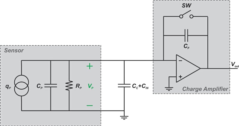
Figure 4. A schematic showing a charge amplifier, using a reset switch, in configuration with a sensor.
Before making a measurement, the switch is turned on to discharge the feedback capacitor and set the DC voltage of the inverting input of the op-amp. Then, the switch is turned off to start the measurement phase, as seen in Figure 5.
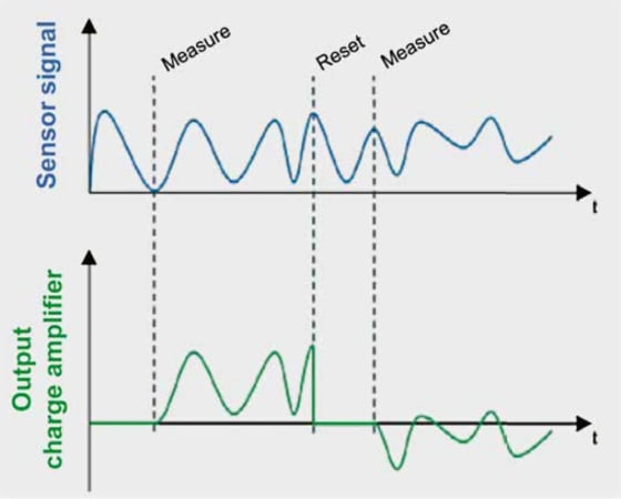
Figure 5. The circuit operation of the charge amplifier. Image used courtesy of Kistler
Again, the upper curve shows the charge produced by the sensor, and the lower curve depicts the output of the charge amplifier. Note that, when the switch is on, the output is zero. As a result, the reset switch also fixes the zero point for the subsequent measurement.
Although incorporating a reset switch maximizes the time constant, it makes the circuit susceptible to drift phenomenon. Drift refers to a change in the output of the charge amplifier that occurs over a period of time and is not caused by a change in the physical parameter being measured (acceleration in our discussion). Drift is caused by several different non-ideal effects such as the input bias current and offset voltage of the op-amp.
To further this discussion, the effect of the feedback resistor on the amplifier’s low-frequency response and drift behavior should be evaluated in greater detail.
To see a complete list of my articles, please visit this page.
Related Content