 Facebook
 Google
 GitHub
 Linkedin
Improving Phase Accuracy Using a Composite Op-Amp
This is the final part of a six-article series on composite amplifiers. In this last part, we'll show how to improve phase accuracy.
In Part 1 of a six-article series on composite amplifiers we investigated how to boost the output current drive capability of an op-amp and in Part 2, we discussed PSpice verification for our resulting voltage buffer. In Part 3, we showed how to extend the closed-loop frequency bandwidth, in Part 4 how to increase the slew rate, and in Part 5 how to achieve higher DC precision.
In this last article, we are about to show how to improve phase accuracy.
As in the last article, we'll refer back to two figures from Part 1 of the series.
The block diagram of Figure 1:
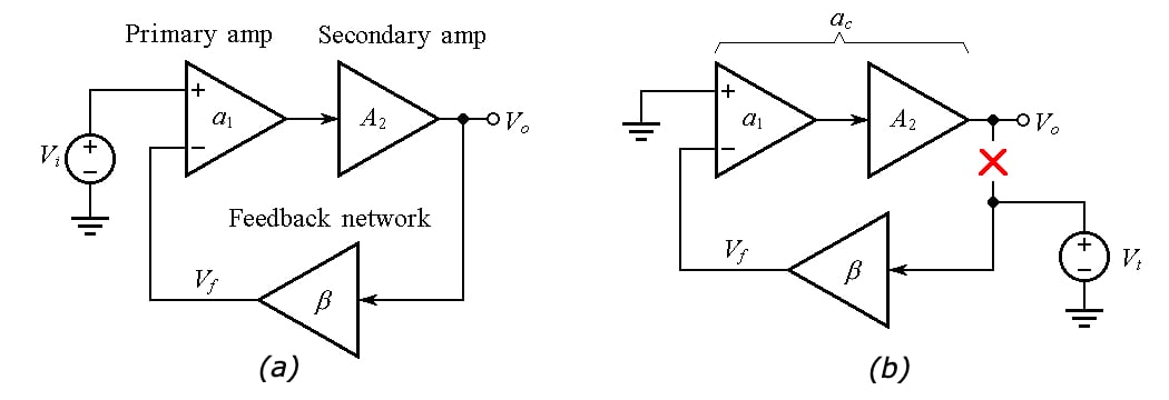
Figure 1. (a) Block diagram of a composite voltage amplifier. (b) Circuit to find the open-loop gain ac and noise gain 1/β of the composite amplifier.
Rate-of-closure (ROC) possibilities:
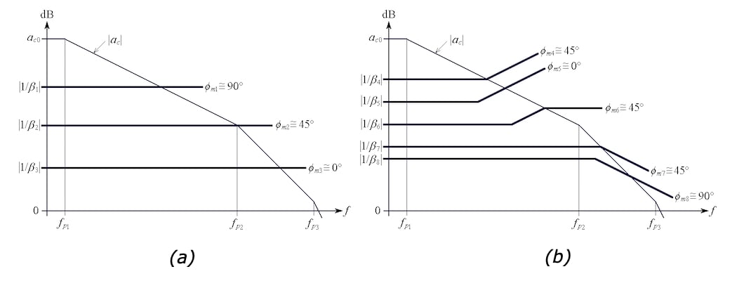
Figure 2. (a) Frequently encountered phase-margin situations with (b) frequency-independent and (b) frequency-dependent noise gain 1/β(jf).
Now, let's move on to how we can improve the phase noise accuracy of a composite amplifier.
Phase Accuracy Applications
There are applications such as SONAR and LiDAR in which the phase relationship between two signals provides important information. In order to minimize phase-measurement errors, the amplifier circuitry processing each signal must exhibit a flat phase response over the signal’s frequency range.
To get an idea, let’s start out with the popular noninverting op-amp configuration of Figure 3(a).
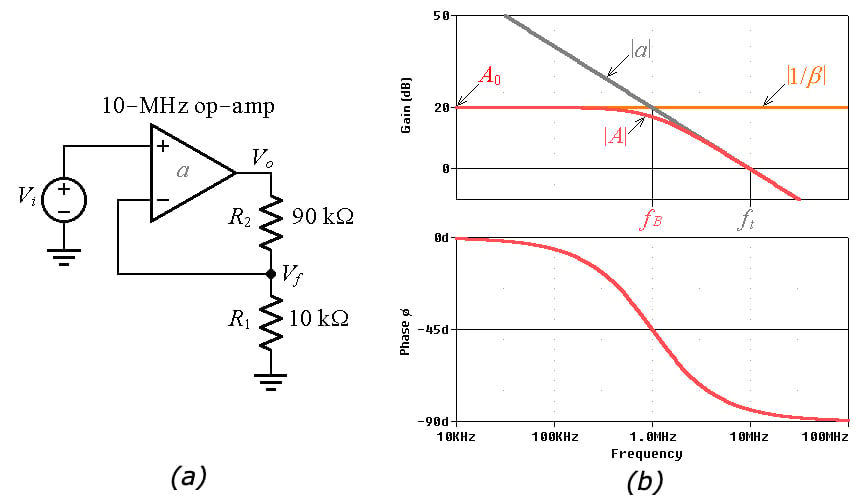
Figure 3. (a) A gain-of-10-V/V noninverting amplifier using an op-amp with a constant gain-bandwidth product (GBP) of 10 MHz. (b) PSpice-generated Bode plots of magnitude and phase.
As we know, the parameter
\[\beta = \frac {V_f}{V_o} = \frac {R_1}{R_1 +R_2} = \frac {1}{1+R_2/R_1}\]
Equation 1
is called the feedback factor, and its reciprocal
\[\frac {1}{\beta} = 1+ \frac {R_2}{R_1}\]
Equation 2
is called the noise gain.
For our circuit, 1/β = 10 V/V, or 20 dB. Moreover, if we denote the closed-loop gain as \(A = V_o/V_i \), the latter’s dc value is \(A_0 = 1/\beta \).
With reference to Figure 3(b), top, the frequency at which the noise gain |1/β| intersects the open-loop gain |a| is called the crossover frequency. Presently, this frequency represents also the closed-loop –3-dB frequency bandwidth \(f_B\). Exploiting the constancy of the GBP on the |a| curve we write \((1/\beta) \times f_B = 1 \times f_t \), so
\[f_B = \frac {f_t}{1+R_2/R_1}\]
Equation 3
where \(f_t\) represents the op amp’s transition frequency. In Figure 3(b), \(f_t\) = GBP = 10 MHz, so \(f_B\) = 1 MHz.
The parameter \(f_B\) is also called the pole frequency. Its presence causes the output \(V_o\) to experience a frequency-dependent phase lag ɸ with respect to the input \(V_i\) such that
\[\phi(f) = -tan^{-1} \frac {f}{f_B}\]
Equation 4
The corresponding plot is shown in Figure 3(b), bottom. It is apparent that this circuit provides an almost flat phase response only up to, say, 10 kHz, where Equation 4 gives \(\phi (10^4) = –0.57^\circ \), a small value. Above 10 kHz, ɸ gradually decreases to eventually settle at –90°.
Active Compensation
We would like to extend the flatness of the phase response well above 10 kHz. This we achieve by using a second, identical op-amp \(OA_2\) to establish an additional pole frequency \(f_{B2}\) inside the feedback loop of the primary op-amp, now relabeled as \(OA_1\). See Figure 4(a) below.

Figure 4. (a) Composite amplifier for improved phase accuracy. (b) Idealized circuit for a quick analysis
To develop a basic feel for the circuit, refer to Figure 4(b), where the open-loop gains are assumed to be infinite. As we know, this implies virtual shorts between the input terminals of each op-amp, so all four inputs are at the same potential \(V_i\), as shown. Consequently, the closed-loop dc gain of the composite amplifier is
\[A_{c0} =\lim_{f\rightarrow 0} \frac {V_o}{V_i} = 1 + \frac {R_2}{R_1}\]
Equation 5
We observe also that \(OA_2\) is operating as a noninverting-amplifier, so we apply Equation 3 and express the closed-loop pole frequency of \(OA_2\) as
\[f_{B2} = \frac {f_t}{1+R_4/R_3}\]
Equation 6
We now seek where to position \(OA_2\)’s pole frequency \(f_{B2}\) relative to \(OA_1\)’s pole frequency, rewritten as
\[f_{B1} = \frac {f_t}{1+R_2/R_1}\]
Equation 7
Computer simulation will provide us with an empirical answer.
With reference to Figure 5, a look at the phase plot reveals that the curve with the highest degree of flatness is that corresponding to A2 = 10 V/V, obtained with R4 = 90 k. This implies \(f_{B2} = f_{B1}\), by Equations 6 and 7.
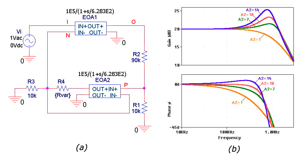
Figure 5. (a) PSpice circuit using Laplace blocks to simulate the 10-MHz op-amps of the composite amplifier of Figure 4(a). (b) Closed-loop magnitude and phase plots for different values of EOA2’s closed-loop gain: A2 = 1 V/V, 7 V/V, 10 V/V, and 14 V/V, obtained with R4 = 0, 60k, 90k, and 130k.
To better understand the role of \(OA_2\) inside \(OA_1\)’s feedback loop, let us break the loop as in Figure 6(a), inject a test voltage \(V_t\), and obtain the noise gain as 1/β = V(T)/V(N). Also, obtain the open-loop gain as a = –V(O)/V(N).
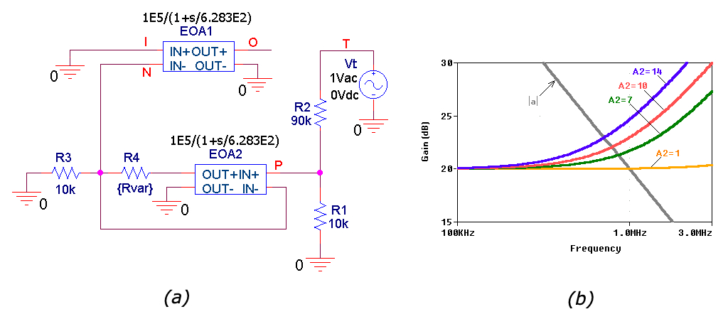
Figure 6. Using PSpice to visualize the plots of OA1’s open-loop gain |a| and noise gain |1/β| for different values of EOA2’s closed-loop gain A2.
Turning next to the plots of Figure 6(b), we note the following. For A2 = 1 V/V, we have a situation corresponding to the \(|1/\beta_1|\) curve of Figure 2(a), indicating a phase margin of \(\phi_m\) ≅ 90°.
Increasing A2 causes the |1/β| curves to bend upwards and to shift leftwards, approaching a situation of the type of the \(|1/\beta_7|\) curve of Figure 2(b), for which \(\phi_m\) ≅ 45°. We are witnessing a gradual decrease in ɸm, in turn, accompanied by a gradual increase in gain peaking, as seen in Figure 5(b), top.
For each |1/β| curve of Figure 6(b) we can find the phase margin as
\[\phi_m =90^\circ -\phi_x\; \]
Equation 8
where \(\phi_x\) is the phase of the |1/β| curve under consideration as measured right at its crossover frequency with the |a| curve. We get the following data: for A2 = 1 V/V, \(\phi_m\) ≅ 84°; for A2 = 7 V/V, \(\phi_m\) ≅ 59°; for A2 = 10 V/V, \(\phi_m\) ≅ 52°; for A2 = 14 V/V, \(\phi_m\) ≅ 45°.
In Figure 7, we compare the desired composite amplifier against the single-op-amp realization.
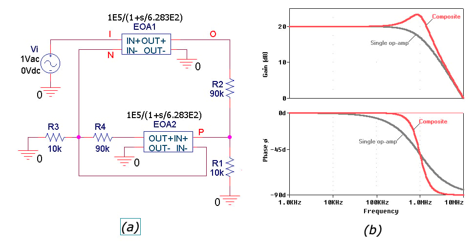
Figure 7. (a) The final composite design, along with (b) its Bode plots.
Using the cursor, we find that at 100 kHz the composite gives a phase of –0.058° versus the single-op-amp phase of –5.7°; at 10 kHz it gives –0.00017° versus –0.57°; at 1 kHz it gives –0.000012° versus –0.057°.
If a maximum tolerable phase error is, say, –1.0°, then the useful frequency range of the composite amplifier extends all the way up to about 260 kHz, whereas that of the single op-amp extends only to 17 kHz.
Finally, the composite’s gain exhibits a peak of 3.33 dB at 862 kHz. Peaking is the price we are paying in order to improve phase accuracy.
I hope this series has helped you greatly expand your understanding of composite amplifiers. If you have additional questions or requests for articles, please share them in the comments below.
Related Content


Hi,
Could it be possible to expand and phase accuracy and frequency bandwith ? What doi you think about that ?
Thanks, Charles