 Facebook
 Google
 GitHub
 Linkedin
Achieving High DC Precision Using Composite Op-Amps
In Part 5 of this series on composite amplifiers, we'll discuss how to achieve higher DC precision.
In Part 1 of this series on composite amplifiers, we investigated how to boost the output current drive capability of an op-amp and then verified our voltage buffer cicrcuit via PSpice simulation in Part 2. In Part 3, we showed how to extend the closed-loop frequency bandwidth, and in Part 4 how to increase the slew rate.
In this article, we'll show how to achieve higher DC precision.
As we progress, we shall make references to Part 1, especially to the block diagram of Figure 1.
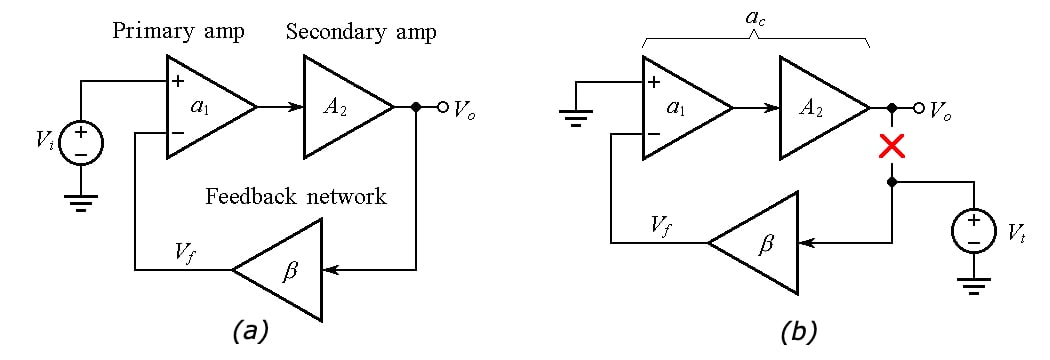
Figure 1. (a) Block diagram of a composite voltage amplifier. (b) Circuit to find the open-loop gain ac and noise gain 1/β of the composite amplifier.
We'll also refer to the rate-of-closure (ROC) possibilities summarized in Figure 2.
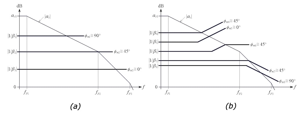
Figure 2. (a) Frequently encountered phase-margin situations with (b) frequency-independent and (b) frequency-dependent noise gain 1/β(jf).
Correlation Between Loop Gain and DC Precision
Let's consider Figure 3 below, which shows the popular noninverting op-amp configuration and its corresponding Bode plot for the open-loop gain, the noise gain, and the loop gain.
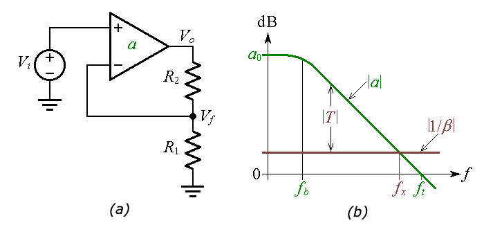
Figure 3. (a) Noninverting op-amp configuration. (b) Bode plot showing the open-loop gain a, the noise gain 1/β, and the loop gain T.
Note that a0 is the DC value of the gain a, fb is the bandwidth, and ft is the transition frequency. The frequency at which |a| and |1/β| intersect is called the crossover frequency fx.
In Figure 3(a), we see the closed-loop gain A of the noninverting op-amp, which takes on the insightful form
\[A = \frac {V_o}{V_1} = A_{ideal} \frac {1}{1+1/T}\]
Equation 1
where
\[A_{ideal} = \lim_{T\rightarrow \infty} A = 1+ \frac {R_2}{R_1}\]
Equation 2
Moreover, T is called the loop gain, and
\[T = a\beta\]
Equation 3
where a is called the open-loop gain, and β is called the feedback factor
\[\beta = \frac {V_f}{V_o} = \frac {R_1}{R_1+R_2}\]
Equation 4
The reciprocal of the feedback factor
\[\frac {1}{\beta} = 1 + \frac {R_2}{R_1}\]
Equation 5
is called the noise gain because this is the gain with which the op-amp will amplify any input noise, such as the input offset voltage \(V_{OS}\). Clearly, for the present circuit we have \(A_{ideal} = 1/\beta \).
Rewriting Equation 3 as T = aβ = a/(1/β), taking the logarithms of both sides, and multiplying by 20 to express in decibels, indicates that we can visualize the decibel plot of |T| as the difference between the decibel plot of |a| and the decibel plot of |1/β|. This is shown in Figure 3(b).
With reference to Equation 1, it is apparent that the term 1/T represents a form of error: in our effort to approximate the ideal gain of Equation 2, we’d like T to be as large as possible: ideally, T → ∞, so A → \(A_{ideal}\).
Achieving High DC Precision at High Noise Gains
As seen in Figure 3(b), the larger the noise gain is, the smaller the loop gain, and thus the lower the precision.
What if the application at hand calls for a high noise gain as well as high DC precision?
For example, suppose we wish to implement a noninverting amplifier with \(A_{ideal}\) = 1,000 V/V (= 60 dB) using an op-amp with \(a_0\) = 100,000 V/V (= 100 dB). This would give a DC loop gain of \(T_0\) = 100 – 60 = 40 dB, or \(T_0\) = 100, indicating a DC error of about 1%, by Equation 1.
What if we want to reduce this error significantly?
Clearly, a single op-amp won’t do it, so let us cascade two of them, as in Figure 4(a).
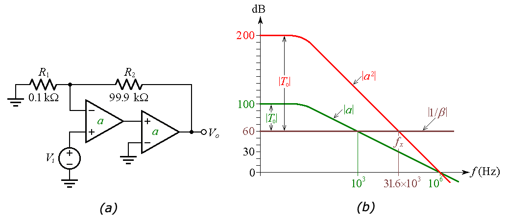
Figure 4. (a) Cascading two op-amps to achieve a composite open-loop gain of a×a = a2. (b) Bode-plot visualization. The crossover frequency changes from 103 Hz to fx = (103×106)1/2 = 31.6×10³ Hz.
The ensuing composite amplifier will sport an open-loop gain of \(a \times a = a^2\), whose magnitude plot we construct point-by-point by doubling that of a.
As depicted in Figure 4(b), we now have \(T_0\) = 200 – 60 = 140 dB, or \(T_0 = 10^7\), for a DC error of 0.1 parts-per-million, quite an improvement. Unfortunately, the price we are paying for this is outright instability!
In fact, while the single-op-amp circuit conforms to the \(|1/\beta_1|\) curve of Figure 2(a), for a phase margin of \(\phi_m \approx 90^\circ \), the composite device conforms to the \(|1/\beta_3|\) curve of Figure 2(a), with \(\phi_m \approx 0^\circ \).
Clearly, our composite needs frequency compensation.
Frequency Compensation
Lacking the ability to modify the \(|a^2|\) curve, we must focus on suitably modifying the |1/β| curve.
A common strategy is to aim for \( \phi_m = 45^\circ \), in conformance with the \( |1/ \beta_7| \) curve of Figure 2(b). This we achieve by placing a suitable capacitance \(C_f\) in parallel with \(R_2\), as depicted in Figure 5(a). While leaving the \(|1/ \beta | \) curve unchanged at low frequencies, the presence of \(C_f\) introduces a breakpoint at the frequency at which the impedance presented by \(C_f\) equals, in magnitude, \(R_2\).
For \(\phi_m = 45^\circ \) we wish this frequency to be the crossover frequency \(f_x\), so we impose \(|1/(j2\pi f_x C_f)| = R_2 \) and get
\[C_f = \frac {1}{2 \pi f_x R_2}\]
Equation 6
With the values of \(R_2\) and \(f_x\) of Figure 5, we get \(C_f\) = 50.38 pF. Denoting the closed-loop gain of the composite amplifier as \(A_c\), we observe that besides the dramatic improvement in DC precision, we also have a closed-loop bandwidth expansion from 1 kHz to 31.6 kHz.
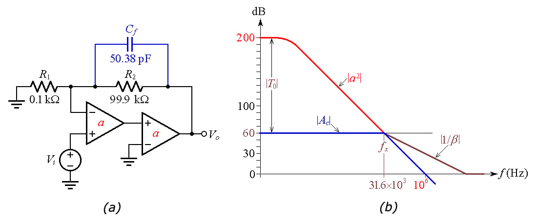
Figure 5. Frequency compensation of the composite amplifier of Figure 4 for ɸm = 45°.
The closed-loop AC response of an amplifier that has been compensated for \(\phi_m = 45^\circ \) exhibits peaking. If peaking is undesirable, we can compensate for \(\phi_m = 65^\circ \), which marks the onset of peaking.
This requires that we suitably lower the breakpoint frequency, now denoted as \(f_1\) in Figure 6(b).
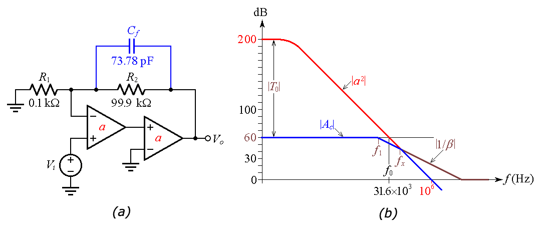
Figure 6. Frequency compensation for ɸm > 45°.
How do we find the necessary \(f_1\)?
Considering that \(a^2\) gain contributes –180°, \(\phi_m\) will coincide with the phase contribution of \(f_1\) at \(f_x\), or
\[\phi_m = tan^{-1}\frac {f_x}{f_1}\]
Equation 7
Applying simple geometric reasoning, we note that \(f_0\) is the geometric mean of \(f_1\) and \(f_x\), or
\[f_0 = (f_1 \times f_x)^{1/2}\]
Equation 8
Eliminating \(f_x\), we find, after minor algebraic manipulation,
\[f_1 = \frac {f_0}{\sqrt{tan \phi_m}}\]
Equation 9
So, for \(\phi_m = 65^\circ \), our circuit needs \(f_1\) = 21.58 kHz, which we achieve by raising the \(C_f \) of Figure 5(a) by a factor of 31.62/21.58 to obtain the value of 73.78 pF shown in Figure 6(a).
Verification Using PSpice Simulation
We can readily verify the calculations performed above by means of computer simulation. The PSpice circuit of Figure 7 has been set up to simulate the cases \(\phi_m\) = 0°, 45°, and 65°. For \(\phi_m\) = 0°, the circuit exhibits almost infinite peaking, indicating a circuit on the verge of oscillation.
(When implemented with real-life components, the circuit is guaranteed to oscillate because of the additional phase lag due to higher-order pole frequencies not accounted for in our simplified op-amp model.)
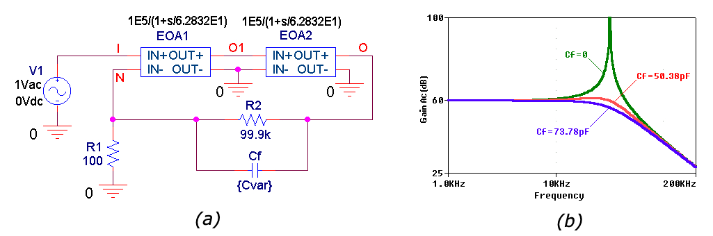
Figure 7. (a) PSpice circuit of a high-DC-precision, 60-dB-gain composite amplifier using Laplace blocks to simulate 1-MHz op-amps. (b) Closed-loop AC gains for phase margins of about 0°, 45°, and 65°.
The closed-loop gain corresponding to \(\phi_m ≅ 45^\circ \) exhibits a bandwidth of \(f_B = 40.3 kHz \), whereas with \(\phi_m ≅ 65^\circ \) we have \(f_B = 30.5 kHz \). If a lower bandwidth is desired (for instance to reduce noise) one can increase \(C_f\), but only up to a point.
Increasing \(C_f\) shifts the |1/β| curve of Figure 6(b) further to the left, bringing its horizontal-axis breakpoint closer to the crossover point. If this breakpoint is moved to the left of the crossover frequency, we run again into \(\phi_m ≅ 0^\circ \) and the circuit will be on the verge of oscillation.
In Part 6, we will show how to improve phase accuracy.


We wanted to as kyou MANY times - make these articles downloadable, in format OTHER than buggy/complex webpage [html].
I.e. make it downloadable as a *.PDF file or similar !