Facebook
 Google
 GitHub
 Linkedin
Introduction to Double Data Rate (DDR) Memory
Learn about double data rate (DDR) memory key concepts and applications surrounding this digital communication technique, where two data words are transferred during one clock cycle.
Serial data transfer has important advantages over parallel data transfer, and in many systems, these advantages are significant enough to justify adding circuitry that serializes and deserializes parallel data so that it can be transmitted as serial data. Computer memory, however, is one application area in which parallel data transfer is still prevalent. Since they can read and write many digital signals simultaneously, parallel interfaces are fast, and designers are always looking for ways to make them even faster.
An old but still relevant technique for achieving a major increase in data-transfer rate is called double pumping, and this feature is what turns a memory system into a double data rate (DDR) memory system. A “single-pumped” memory system adopts the time-honored strategy for synchronously moving data from one IC to another. Basically, logic signals change once per clock cycle and are sampled by the receiver on either the rising edge or the falling edge of the clock. In this scheme, the rate at which words are transferred cannot exceed the clock frequency.
For example, if your clock runs at 133 MHz, you can (ideally) transfer 133 million words per second. Note that the bit transfer rate depends on the system architecture since different computing systems use different word lengths—8 bits, 16 bits, etc. A double-pumped system could achieve 266 MT/s (millions of transfers per second) with a 133 MHz clock.
In this article, we'll take a look at the differences between single and double data rate interfaces, why we use DDR, and its applications.
SDR vs. DDR: Single Data Rate and Double Data Rate Interfaces
The timing diagram shown below in Figure 1 is an example of a single data rate memory interface.
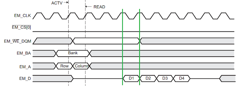
Figure 1. Example of a single data rate memory interface. Image [modified] used courtesy of Texas Instruments
First, the memory bank is selected using the EM_BA signals, and the row and column addresses are established by the EM_A signals. Data words D1, D2, D3, and D4 are output on the EM_D pins. Notice how one data word occupies an entire cycle of the EM_CLK signal.
The next timing diagram (Figure 2) we'll take a look at depicts a double data rate interface.
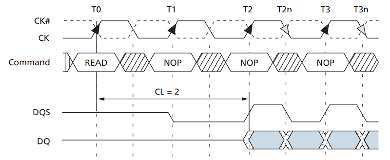
Figure 2. An example of a double data rate interface. Image used courtesy of Micron
The “DQ” line represents the data signals, and the unshaded X-shaped areas between shaded areas denote transitions from one word to the next. You can see that each word requires only half of a full clock cycle. Keep in mind that this chip uses a differential clock, which is why the timing diagram has a CK signal and a complementary CK# signal.
The Motive: Why Double Data Rate?
You might wonder why engineers went through the trouble of creating new logic for DDR signaling when they could have increased the clock frequency by a factor of two. The primary explanation for this decision is contained in two words representing countless hours of high-speed R&D: signal integrity.
High-frequency signals—where “high frequency” is understood relative to the constraints of a given technological era or application scenario—are a source of much consternation for board designers. These signals:
- Suffer more dispersion caused by limited channel bandwidth
- Require more power consumption
- Are more susceptible to capacitive coupling and reflection,
- Radiate more efficiently from the various unintentional antennas present on any PCB
They’re also more difficult to characterize and troubleshoot using test equipment. An oscilloscope, for example, has limited analog and digital bandwidth, and it will introduce more distortion into a waveform as frequency increases.
Thus, it makes sense to extract as much throughput as possible from the existing clock rate before attempting to implement a higher clock rate. By moving from a single data rate interface to a DDR interface, designers can significantly increase the data transfer rate without changing the system’s maximum signal frequency. All of this can be accomplished even though the maximum frequency of the data signals has increased by a factor of two this new data frequency is not higher than the previous clock frequency.
DDR Memory Applications
Double pumping is a generic feature that has been used in various parallel data transfer interfaces. Even high-speed data converters have adopted this technique. In the analog-to-digital converter (ADC) timing diagram shown in Figure 3, for example, one sample is digitized in the time required for one full clock period, but the digital outputs use DDR timing because two data bits are multiplexed onto each output.
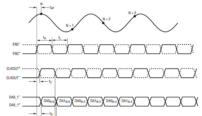
Figure 3. Example ADC timing diagram where all the signals shown are differential. Image used courtesy of Analog/Linear Technology
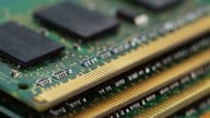
However, DDR parallel transfer is still closely associated with SDRAM (synchronous dynamic random-access memory) used in computing systems. For decades, engineers have been hard at work increasing the speed at which computers can move and process digital data, and DDR signaling allowed them to double throughput while maintaining whatever maximum clock frequency was feasible at the time.
First-generation DDR SDRAM, released in 1998, supported clock frequencies up to 200 MHz and corresponding transfer rates up to 400 MT/s. Then came DDR2, DDR3, DDR4, and finally, DDR5, which is what we’re currently using. DDR5 has maximum transfer rates exceeding 7 GT/s.
Laying the Groundwork in DDR Memory
The development of DDR computer memory was a relatively lengthy process, which testifies to the many complexities and design challenges that we didn’t examine in this introductory article. Nevertheless, I hope that you now understand the basic premise of DDR digital communication. If you’d like to learn more about digital memory, here are some other resources that might interest you:
- Digital Memory Terms and Concepts
- DRAM, SRAM, FLASH, and a New Form of NVRAM: What’s the Difference?
- The Ripple Effects of Robert H. Dennard, Inventor of DRAM and Dennard Scaling
Related Content