 Facebook
 Google
 GitHub
 Linkedin
Learn About Three-Op Amp Instrumentation Amplifiers
In this article, we'll discuss instrumentation amplifiers (in-amps) which have high common-mode rejection and provide high and equal input impedances. We will also look at the advantages and disadvantages of a commonly-used in-amp often referred to as the three-op amp in-amp.
In previous articles in this series, we discussed that instrumentation amplifiers (in-amps) should have a high common-mode rejection as well as high and equal input impedances to successfully extract a small differential signal.
In this article, we’ll look at a commonly-used in-amp often referred to as the three-op amp in-amp. We’ll see that a three-op amp in-amp employs a clever architecture with several interesting features.
The Classic Three-Op-amp In-amp
A commonly used in-amp circuit that provides a high CMRR along with balanced, high input impedances is the three-op amp structure depicted in Figure 1.
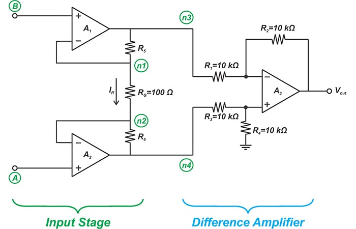
Figure 1
The above schematic can be decomposed into two sections. The input stage acts mainly as a buffer. The output stage is a difference amplifier discussed in the previous article. As we’ll see below, the three-op amp in-amp employs a clever architecture with several interesting features.
High, Balanced Input Impedance
Both nodes A and B are connected to the non-inverting input of the corresponding op amps. This gives high, balanced input impedances without resorting to complicated feedback techniques.
The Input Stage Can Provide High Differential Gain and CMRR
Let’s first calculate the differential gain of the input stage. The negative feedback along with the high gain of the op amps will force both the inverting and non-inverting inputs of A1 and A2 to have the same voltage. Hence, we have:
\[v_{n1}=v_B\]
\[v_{n2}=v_A\]
The current through RG, and hence through R5 and R6, will be:
\[I_R=\frac{v_{n1}-v_{n2}}{R_G}=\frac{v_B-v_A}{R_G}\]
Therefore, with R5=R6, the voltage difference at the input of the difference amplifier will be:
\[v_{n3}-v_{n4}=(R_5+R_G+R_6) \times I_R=(2R_5+R_G) \times \frac{v_B-v_A}{R_G}\]
which simplifies to
\[v_{n3}-v_{n4}=\left ( \frac{2R_5}{R_G}+1 \right )\times (v_B-v_A)\]
Equation 1
We know that the gain of the difference amplifier is:
\[v_{out}=\frac{R_2}{R_1}(v_{n4}-v_{n3})\]
Hence, we have:
\[v_{out}=\frac{R_2}{R_1}\left ( \frac{2R_5}{R_G}+1 \right )\times (v_{A}-v_{B})\]
Therefore, the total differential-mode gain of the circuit is:
\[A_d=\frac{R_2}{R_1}\left ( \frac{2R_5}{R_G}+1 \right )\]
Equation 1 shows that the differential gain of the input stage, Ad1, can be adjusted by choosing the value of R5 and RG. For example, with the typical values in Figure 1 and R5=50 kΩ, Ad1 will be:
\[A_{d1}=\frac{v_{n3}-v_{n4}}{v_B-v_A}= \frac{2R_5}{R_G}+1=\frac{2 \times 50 k \Omega}{100 \Omega}+1=1001\]
Equation 2
What would be the common-mode gain of the input stage? Based on the above analysis, with vA=vB, the voltage across RG will be zero. Hence, no current will flow through R5, RG, and R6; and we have:
\[v_{n3}=v_{n4}=v_A=v_B\]
To summarize, the input stage can give us a large differential gain while passing the common-mode signal at unity gain. This leads to a relatively high CMRR at the input stage. Next, the difference amplifier will further suppress this residual common-mode signal. An interesting property of the input stage is that increasing the differential gain also increases the CMRR.
Adjust the Gain by Setting the Value of a Single Resistor
As you can see from Equation 1, we can adjust the differential gain of the in-amp by adjusting the value of a single resistor RG. This is important because unlike the other resistors in the circuit, the value of RG does not need to be matched with any other resistor.
For example, if we attempt to set the gain by changing the value of R5, we’ll also need to change R6 accordingly. Implementing matched, adjustable resistors is more challenging than adjusting a single resistor.
The Source Resistance Doesn’t Appear in the Gain Equation
Consider the bridge measurement system depicted in Figure 2 below.
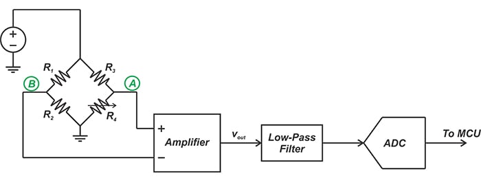
Figure 2.
Applying Thevenin's theorem, we can model the bridge as shown in Figure 3.
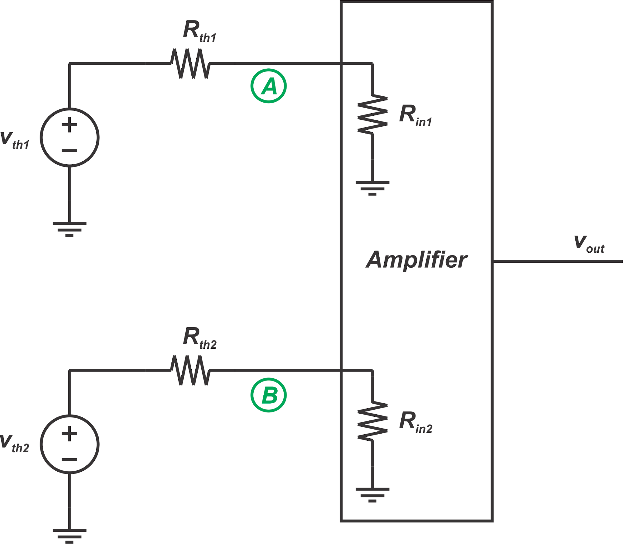
Figure 3.
Here, Rth1 and Rth2 are the equivalent resistances of the two bridge branches; and Vth1 and Vth2 are the Thevenin equivalent voltages of nodes A and B. Besides, the above figure models the impedances “seen” at the amplifier inputs by Rin1 and Rin2.
This model shows that a voltage divider is created by the input impedance of the amplifier and the equivalent resistance of the bridge. This voltage divider determines the voltage that appears at the input of the amplifier. Hence, with a gain stage such as the difference amplifier, that has a relatively small input impedance, the overall gain will be a function of Rth1 and Rth2. This leads to a poor gain predictability and reduces the accuracy.
However, the three-op amp in-amp provides very high impedances at its inputs. Hence, the Thevenin equivalent voltage of the bridge appears at the amplifier input without being attenuated by the voltage dividers. Since the source resistance does not appear in the gain equation, we have a more predictable gain and higher accuracy.
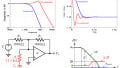
Reduced Common-Mode Voltage Range
One limitation of the three-op amp in-amp is that the input common-mode range can be limited if we try to achieve a very high differential gain at the input stage.
As shown in Figure 4, when a differential-mode signal of vd that is running on a common-mode voltage of vc is applied to the inputs, the voltage at nodes n3 and n4 will be \(v_c-A_{d1}\frac{vd}{2}\) and \(v_c+A_{d1}\frac{vd}{2}\), respectively. Here, Ad1 is the differential gain of the input stage given by Equation 2 above.
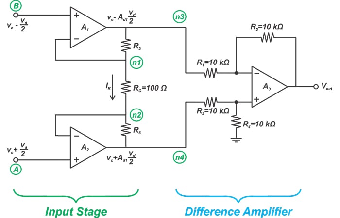
Figure 4
With vd=10 mV and Ad1=1000, the voltage at node n4 will be vc+5V. This voltage should be in the common-mode range of the output amplifier, A3, so it does not saturate. As you can see, depending on the differential-mode gain of the input stage, we need to set an upper limit on the input common-mode voltage vc.
Conclusion
A three-op amp in-amp is a commonly-used structure that can amplify the differential signal while stripping off any common-mode voltage. An advantage of this circuit is that a single resistor that doesn’t need to be matched with any other resistor in the circuit determines the gain. This allows us to more easily adjust the circuit gain. Besides, with a three-op amp in-amp, the source impedance does not play a role in calculation of gain.
These advantages are achieved at the cost of extra signal delay and reduced common-mode voltage range.
To see a complete list of my articles, please visit this page.


Good n perfect knowledge
Congratulations ! The matter it’s important and the presentation it’s really good.
Hi, I liked the article. One comment that would make the below statement from your article more clear is that CMRR = (differential gain/common mode gain) by definition, so that if you increase the numerator and keep the denominator the same, then the whole fraction, the CMRR, will also increase.
Your article states: “To summarize, the input stage can give us a large differential gain while passing the common-mode signal at unity gain. This leads to a relatively high CMRR at the input stage. Next, the difference amplifier will further suppress this residual common-mode signal. An interesting property of the input stage is that increasing the differential gain also increases the CMRR.”