Facebook
 Google
 GitHub
 Linkedin
Simulating an Op-Amp’s Offset Voltage Variation
In this article, we’ll create an LTspice circuit for analyzing the effect of unpredictable offset voltage on the performance of a precision current-source circuit.
Nowadays, we can often find op-amps with typical offset voltage that is very low relative to system requirements. If one of these op-amps fits in the project budget, we will have little if any need to consider offset voltage during the design process.
Sometimes, though, this non-ideal aspect of op-amp operation can influence a circuit’s performance in noticeable ways. My objective in this article is to present a method of analyzing the effects of offset voltage by means of SPICE simulation.
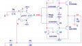
The circuit that I’ll use as an example is the precision current pump that I explored in three previous articles. The diagram below provides the schematic for this circuit and the theoretical input-output relationship.
Diagram of a precision current pump. Image used courtesy of Analog Devices
What is Input Offset Voltage?
Inevitable component mismatches inside an op-amp cause a 0 V differential input to produce a non-zero positive or negative output voltage. The input offset voltage is the voltage that you must apply to one of the input terminals in order to compensate for the mismatches and thereby achieve 0 V output for 0 V input.
Offset voltage is problematic because it causes an op-amp to deviate from the idealized model that produces better results and is more user-friendly. Furthermore, the severity of this deviation cannot be predicted with high precision: a datasheet can describe offset voltage using a single number only if it is referring to the typical or maximum offset voltage.
To get a more complete picture of offset-voltage behavior, you need to look at the distribution obtained when numerous devices (of the same part number) are characterized.
In the previous article on simulating current-pump performance with tolerance and temperature, I used the AD8606 op-amp for my current-pump simulations. The AD8606 datasheet provides the following plot to help us understand the distribution of offset-voltage values for this part number:
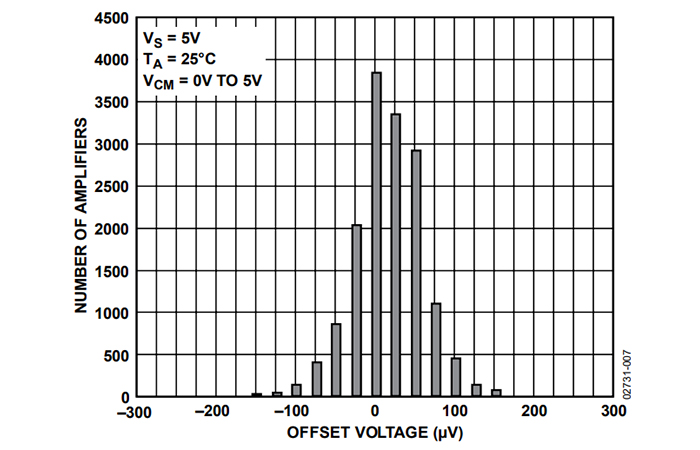
Plot taken from the AD8606 datasheet. Image used courtesy of Analog Devices
The shape of the distribution resembles the shape of the normal (aka Gaussian) distribution, and that’s not surprising, because we expect a normal distribution when a measured value is influenced by multiple randomly varying parameters.
Modeling Input Offset Voltage
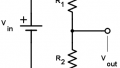
If we want to incorporate offset voltage into our circuit analysis, we add a DC voltage source in series with the positive or negative input terminal of the op-amp. The result is a circuit model that will look something like this:
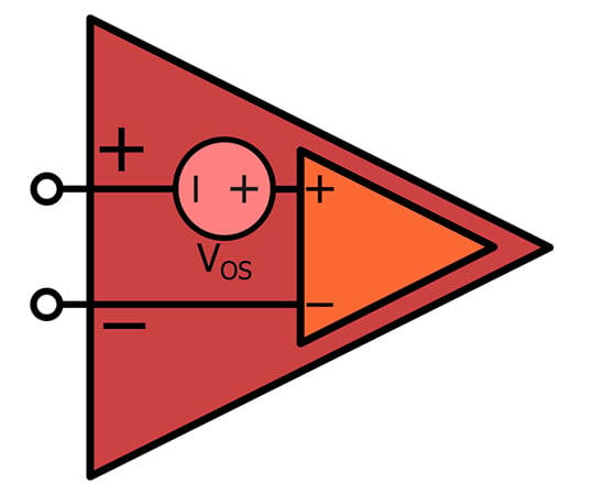
The orange op-amp is an ideal op-amp, or at least an op-amp with no offset voltage. The red op-amp represents the “more realistic” op-amp that we have created by combining the ideal op-amp with a DC voltage source.
The value of the voltage source would usually be the typical offset voltage or the maximum offset voltage—if you have to choose a single value. In a SPICE simulation, we can choose many different values.
Simulating the Effect of Offset Voltage
In previous articles, we used LTspice’s Monte Carlo (abbreviated mc) function to produce variations in resistance values corresponding to a resistor’s tolerance. The mc function, however, produces random numbers according to the uniform distribution. We want random numbers with a normal distribution, so we’ll use the gauss function instead. Here’s the circuit:
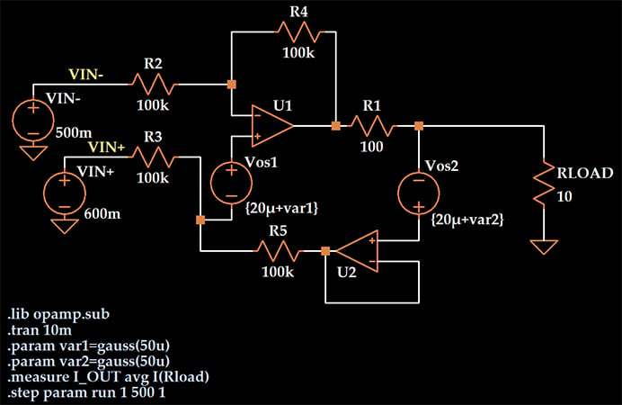
My intention here is to analyze only the effect of the offset voltage. All of the resistors are set to their nominal value with no tolerance, and the op-amp is LTspice’s ideal single-pole op-amp rather than a macromodel corresponding to a real component.
I want the offset voltages to reflect the variation that we might see in a real op-amp, and since I used the AD8606 in a previous simulation, I decided to design this simulation according to the AD8606’s offset-voltage characteristics. In other words, I attempted to approximate the offset-voltage distribution conveyed by the histogram that we looked at earlier in this article.
The AD8606 datasheet gives 20 μV as a typical offset-voltage value, so I used that as the nominal value for the voltage supplies that represent offset voltage. The argument passed to the gauss function is the standard deviation of the randomly generated numbers. Thus, my offset-voltage values are defined as {20μ + gauss(50μ)}, meaning a Gaussian distribution with a mean of 20 μV and a standard deviation of 50 μV.
As we’ll see in the next article, this combination of mean and standard deviation results in a distribution that is reasonably consistent with the histogram reported for the AD8606. This same technique could be used to approximate the offset-voltage specs of any op-amp part number that has an approximately normal distribution of offset-voltage values—you just change the mean and/or standard deviation as necessary.
Conclusion
We’ve prepared an LTspice schematic that will allow us to predict the influence of offset voltage on the precision of a constant-current-source circuit. We’ll continue this discussion and look at some simulation results in the next article.
Related Content