Facebook
 Google
 GitHub
 Linkedin
Op Amps Characteristics (Part 2) - Internal Circuitry
Video Lectures created by Tim Feiegenbaum at North Seattle Community College.
We're continuing in 11.1 and we're looking at the internal circuitry of an op amp.
Op amps are composed of standard components such as—notice—transistors, resistors, diodes, and so forth, and a capacitor right here.
The input terminals of an op amp are connected to the bases of transistors. If we look at this, we'll see … Here we had the two input terminals. Here is the negative voltage and the positive voltage. This was pin six, the output, and then this was the offset, pins one and five go here. When we see an op amp, we just see the input pins; we don't see all of this circuitry and the details of what's going on in the circuitry goes well beyond an introductory course.
I do want to mention just a couple of things. You'll notice here if you look at this, this looks kind of like a differential amp here, when you had the two inputs, remember from the last chapter we looked at a differential amplifier? When they integrate components, something that happens is … For example, this component right here, though it looks like a transistor, and it is a transistor, it is doing the same job as a resistor.
This is actually the current regulator that feeds the current into the differential amplifier. The reason they do that is they found that they can make transistors much smaller than a resistor and so, in many cases, the transistors that you'll see in this circuit are actually acting as resistors.
Then I did want to point out the pins one and five, these were the offset values, and you'll notice that one is connected here and the other is connected here. What this is, this is the final output from the differential input and so you have the input coming in here and the input coming in here and, what is commonly done if these are used, a variable resistor can be placed across here and this is usually going to be external to the op amp and disconnected to these two pins and then if there is an offset voltage, that resistance can be varied so that the output voltage can be nulled out.
This is a simplified schematic diagram of what we just looked at. This makes it a little easier to comprehend. Remember, this would be that resistor that controls the current into the differential amplifier. These are the inverting and non-inverting inputs coming into the differential amp and then the output is fed over here. You may recognize this, this looks like the Darlington pair that we looked at in transistor circuits.
In this case, I should mention this also, this would be resistor controlling current, this is the dif amp, this would also be akin to the collector resistor that we looked at in the differential amp that develops the voltage. Then it's going to be fed here into the Darlington amp and from here there is actually a common emitter. This would be the common emitter transistor and this would be the resistor for the common emitter amp, so, again, we have another amplifier here. Then that is fed into a class B configuration and we haven't looked at that.
What's going to happen, as the signal is amplified, the positive signal will come out of Q9 and the negative will come out of Q10. The advantage of this kind of configuration is that the output here can be set for 0 V. Remember that we have the positive and the negative voltages in op amp, and so say we had +15 here and -15 here, the output, at least in theory, could swing from +15 to -15, this would make for a very large potential output.
Again, that is ideal. When we actually use these servers we wouldn't be able to go that, maybe would go to maybe 12-13 V maximum. At any rate, we're going to be able to maximize the output signal swing by use of this particular configuration.
If you're inclined to look at the actual components in the 741 op amp, there's a link right here that you can go to at Wikipedia and they show the actual components in an op amp, though it goes well beyond where we plan to go for this particular course.
Common Chip Connections
This is a common chip connection. In fact, this is the actual op amp as you would see it. In fact, sometimes they come in a cylinder-type configuration. This is commonly the configuration you'll see in a 741. This is the pin layout that you would see, so that little notch right there is right there. As we look at this, this would be pins one, two, three, four, and then five, six, seven, eight, kind of like that. If you were building this, this is the actual component you would be dealing with.
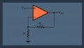
Input Bias Current and Input Resistance
The input bias current of an op amp is considered to be one-half the sum of the two input currents applied.
Op amps using bipolar transistors typically have bias currents in the tens to hundreds of nanoamperes, so it's extremely small.
Op amps are available with FET and MOSFET inputs that have much lower input currents. What are we talking about here? This particular formula is not in your books, but it is stated in your book, the information that's in it. It says, “The input bias current of an op amp is considered to be one-half the sum of the two input currents supplied.” If you added current through the base of Q1 plus the current through the base of Q2 and divided that by two, that would be the average of the two input currents.
What is this talking about? Remember, in our differential amp, we had back in transistor chapter, we had a current that came through the biasing resistor and that current was split two ways and went into the two transistors and most of the current went into the collectors. However, there was that tiny current that actually went out through the base. This current is very small.
In fact, notice here, we're talking tens to hundreds of nanoamperes. A common … I've seen 70 … If we were using this formula here and we were actually measuring the actual currents … And these, by the way, are designed to be matched so that the currents will be close to equal but reality is that they're not exactly equal. So if one was 70 nanoamperes, the other was 90, we'd divide that, we'd say there's maybe 80 nanoamperes of current flowing through the bases of the input into your op amp. You might say to yourself, “It's so tiny, what difference could it possibly make?”
The difference is, that if there is a resistor in the input path here, that tiny current flows across this resistor and it did that, what was the voltage? This voltage is typically extremely small, down in probably microvolts. However, when you consider that the op amp typically has a gain of 100,000, suddenly, this tiny little voltage can become very large and this is where we can get the things like the output offset voltage.
Commonly, in op amp designs, on the input you'll see a resistance here and then they'll have another resistance here that will appear to have no apparent purpose, but its purpose is to equalize those voltages that may be developed from those tiny input currents.
An ideal op amp has infinite input resistance and zero input current. Ideally, remember these are so tiny we say that ideally there isn't input current—actually, there is a little bit. We say that it has infinite input resistance and we also mentioned that in the previous section, that it has a gigantic input, especially if you're using the FET or MOSFET variety of an op amp, and that's one of the reasons in some cases those are preferred, because they have just astronomical input … just hundreds of megohms of input impedance and the currents that they have are going to be much smaller than this, this is a bipolar value that we're looking at here. At any rate, infinite input impedance, zero input incurrent, ideally.
We've looked at input bias current and resistance, we've looked at the chip connections, looked at a simplified diagram and, again, I don't expect you to know all this but this just gives you an idea of what's going on within this device, this is a more detailed one from your text.
That concludes this portion of 11.1.