 Facebook
 Google
 GitHub
 Linkedin
CCD Binning in Imaging Systems: Increasing Signal-to-Noise Ratio and Frame Rate
This article explains a technique that allows us to incorporate flexibility into the operational parameters of a CCD imaging system.
In this article, we'll discuss the concept of binning in CCDs (charge-coupled devices).
This is Part 8 of an ongoing series on CCD image sensors. You can catch up on the rest of the series below:
- Introduction to Image Sensor Technology
- CCD Structure and Functionality
- Full-Frame, Interline-Transfer, and Frame-Transfer CCDs
- Clocking Techniques for CCD Readout
- CCD Output Signals
- Sampling, Amplifying, and Digitizing CCD Output Signals
- The Back-Illuminated CCD: Improving Light Sensitivity
What Is Binning? Combining Charge Packets
CCDs, and the engineers who incorporate them into functional systems, are surprisingly adept at keeping thousands or millions of electron bundles from getting mixed up as they make the journey from pixel site to readout amplifier. However, if for some reason we want the charge from one pixel to mingle with the charge from another pixel, the structure of a CCD makes this easy to accomplish.
Intentionally combining light-generated charge from separate pixels is called binning—as though we’re throwing the electrons into a communal bin of some kind.
Let’s consider why we would want to do this.
The Advantages of Binning
The advantages of utilizing binning in CCDs can be broken into two main points:
- Increasing the frame rate
- Improving the signal-to-noise ratio
Increased Frame Rate
One benefit of binning is speed. Binning is like downsampling; the resolution of the image data decreases according to how much binning is performed.
Let’s say that we have a 1000 × 1000 pixel sensor. If we combine two lines into one before activating the horizontal shift register, we will have only 500 lines of data. Thus, the total readout time is reduced by approximately a factor of two.
Then, if we combine two pixels into one during horizontal readout, we create a line width of 500 pixels and reduce readout time by another factor of two. Keep in mind that this is not a crop—the entire image is still represented in the final data set, but with lower resolution.
This technique is useful in a variety of applications that need flexible imaging operation. One example is a digital camera that needs to produce both high-quality still images and low-quality video. Binning offers downsampled image data at high frame rates, and then non-binned readout is used to acquire an individual image at full resolution.

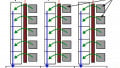
In this diagram, two vertically adjacent pixels are binned, and then two of these binned charged packets are deposited onto the output node, resulting in a binning factor of four.
Improved Signal-to-Noise Ratio (SNR)—And a Bonus Look at Noise Sources in CCDs
Binning is similar to digital downsampling, but not the same. If we downsample by eliminating, for example, every other line and every other pixel, data is simply lost. We’ve reduced resolution, but we haven’t done anything to improve the remaining data.
When we bin, the data isn’t simply discarded, because we are combining the charge of neighboring pixels. This means that binning is a means of increasing SNR in low-light conditions.
It’s important to understand how exactly binning influences SNR, and for that we need to understand the nature of CCD noise. I plan to explore image-sensor noise more thoroughly in a future article, so this will just be the bare bones.
The dominant noise sources in a CCD are photon noise, dark noise, and read noise. Photon noise and dark noise become part of the charge packet generated in each pixel. Read noise includes all noise that is introduced in the process of converting the CCD’s charge packets into usable digital data.
Binning isn’t a solution for photon noise or dark noise; when you combine charge packets from two adjacent pixels, for example, you’re just adding the dark noise of one pixel to the dark noise of another pixel. SNR hasn’t changed.
However, the effect of read noise can be greatly reduced, because the operation of the external electronics is not affected by binning. Those circuits don’t even know that binning has taken place. If you combine two pixels that received equal amounts of incident light, you’ve just doubled the signal, and this combined pixel sees the same amount of read noise during off-chip processing. Thus, SNR has increased by a factor of two. If you bin four pixels, SNR increases by a factor of four.
The Limits of Binning: Don't Exceed Your Full Well Capacity
We can see, then, that binning is a simple and effective means of trading resolution for noise performance. You do have to exercise some degree of restraint, though—this approach to SNR improvement has limits.
Every charge-holding site in the CCD has a full well capacity (AKA well depth) that specifies the maximum number of electrons that can be contained. Vertical binning moves additional electrons—i.e., more than one pixel’s worth—into the horizontal shift register, and horizontal binning moves additional electrons into the output node. If binning introduces a quantity of charge that exceeds the full well capacity, saturation occurs and image quality deteriorates.
Implementing CCD Binning
Let’s briefly look at some timing diagrams that illustrate the relationship between control signals and binning. We’ll use examples from the KAI-1003 CCD image sensor from ON Semiconductor.
The diagram below shows you what standard readout looks like.

Diagram taken from the KAI-1003 datasheet.
The V1 and V2 pulses represent vertical-shift-register activity: lines of pixels are moved toward the horizontal shift register. The V1/V2 pulses are followed by (much-higher-frequency) pulses on the H clocks (H1A, H2A, etc.), which control the horizontal shift register. The R (reset) clock is pulsed once for every H-clock cycle. This is the signal that clears electrons out of the floating diffusion so that the charge packet for the subsequent pixel can be moved in.
The next diagram corresponds to 2×2 binning, i.e., combining a square of four neighboring pixels into one output value.

Diagram taken from the KAI-1003 KAI-1003 datasheet.
V1/V2 are pulsed twice, such that two lines of pixels are combined in the horizontal shift register. This accomplishes vertical binning.
Horizontal binning occurs because there is only one reset pulse for every two H1/H2 pulses—the horizontal shift register deposits electrons from two pixels into the floating diffusion before the charge is cleared.
Conclusion
Binning is a useful technique that allows a CCD to achieve higher frame rates and higher signal-to-noise ratio. I hope that you now understand why imaging systems incorporate binning, how it is implemented, and the limitation imposed by full well capacity.


Binning 4 equal pixel the S/N increase 2 time (noise mean square root)