Facebook
 Google
 GitHub
 Linkedin
Pixel Readout and Frame Rate in CCD Imaging Systems
This article continues our exploration of frame rate in relation to the structure and implementation of a CCD image sensor.
This is part 10 of a series on CCD (charge-coupled device) image sensors. So far, we've talked about the broader concepts of image sensors, introduced the basics of CCDs, and delved into the various types of CCDs (including full-frame, interline-transfer, and frame-transfer). From there, we discussed more granular topics such as CCD readout clocking techniques, CCD output signals, and the sampling, amplifying, and digitizing of those output signals. Most recently, we've discussed back-illuminated CCDs and the concept of using CCD binning to yield better frame rate and signal-to-noise ratio.
In the last article, we introduced the concept of frame rate in CCD image sensors.
I definitely recommend that you read the previous article before this one, as they are essentially two components of the same discussion. But if you really don’t want to, I’ll try not to be offended, and I’ll even attempt to summarize the entire thing in one sentence divided into three bullet points.
Frame rate
- is measured in frames—i.e., individual images—produced per second,
- can be adapted to the requirements of a particular system, and
- is limited by total readout time plus exposure time or, if simultaneous readout and integration is possible, by readout time only.
Frame Rate for an Interline-Transfer CCD
In this section, we’ll use the KAI-2020, a 1600 × 1200 pixel interline-transfer CCD from ON Semiconductor, to take a closer look at the relationship between frame rate and pixel readout.
Pixels vs. Active Pixels
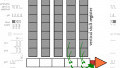
First of all, it’s important to understand that the specified resolution of the sensor does not indicate the total number of pixels that must be transferred to the output node. The KAI-2020 is described as a 1600 × 1200 pixel sensor, but that refers only to the active pixels. As shown in the following diagram, the system must also read out many pixels that will not be included in the final image.
![]()
Dark, buffer, and dummy pixels are not incorporated into this image, but they nonetheless contribute to total readout time. Diagram taken from the KAI-2020 datasheet.
Single vs. Dual Output
Notice how the diagram above has two options for horizontal readout: single output, in which all the pixels in a line are clocked to the left, and dual output, in which half of the line is clocked to the left and the other half is clocked to the right.
This is an important technique for increasing frame rate, because a line can be read out in half the time. It introduces challenges, though: the digital portion of the system must be able to handle two parallel pixel-data streams, and some sort of matching strategy must be implemented to compensate for variations in the two analog signal chains.
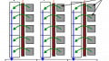
Just in case you’re wondering, two outputs is not the upper limit. For example, the KAF-50100—a 50 megapixel full-frame CCD, also from ON Semiconductor—has four.
![]()
Four-output operation is achieved by incorporating two bidirectional horizontal shift registers. Diagram taken from the KAF-50100 datasheet.
Total Readout Time
To determine the amount of time required to deliver an image, we need to break down the pixel-readout procedure into its distinct phases:
- All of the photodiodes transfer their integrated charge into the vertical shift registers.
- One line is transferred to the horizontal shift register.
- Horizontal clocking causes each pixel in the line to be transferred off-chip via the charge amplifier.
- Steps 2 and 3 are repeated until all pixels from all lines have been read out.
The following diagram provides a visual representation of this process.
![]()
Diagram taken from the KAI-2020 datasheet.
Photodiode charge transfer occurs when V1 is pulsed normally and V2 exhibits the higher-amplitude pulse. This is followed by a delay (tL), and then a normal pulse on V1 and V2 transfers the first line into the horizontal shift register. Next, horizontal readout occurs, then the second line is transferred, then the same horizontal readout occurs, and so on until the end of the image data (in this case, line 1214) is reached.
The diagrams below specify the line timing—i.e., the signal activity that corresponds to the gray-shaded regions representing horizontal readout in the previous diagram.
![]()
![]()
Diagrams taken from the KAI-2020 datasheet.
Though it takes a bit of work, you can accurately calculate the readout duration by adding up every individual element of the readout timing. For example, if the horizontal shift clock has a frequency of 40 MHz, the readout time for one line (tL), with the implementation shown above, is tVCCD + tHD + (25 ns × 1644) + 12.5 ns. If you multiply this by the number of lines and add in the time required for photodiode charge transfer, you know your total readout time and therefore also your maximum frame rate.
Keep in mind, though, that integration time can be ignored only if it is always shorter than the readout time. Specialized applications involving low-light imaging could easily require exposure periods that exceed total readout time.
Factors Affecting Maximum Frame Rate
Even if the datasheet specifies a frame rate, it’s still important to understand the details of readout timing, because the maximum frame rate of your particular application is influenced by a number of operational characteristics. These include the use of binning, the frequency of the clock applied to the horizontal shift register, and the choice of single or dual output.
Also, CCDs such as the KAI-2020 have a “line dump” capability that does pretty much what the name suggests—you can discard an entire line in one fell swoop and thereby avoid all the clock cycles that would be required to transfer the individual pixels through the horizontal shift register. Your maximum frame rate will increase substantially if you’re doing a lot of line dumping.
I personally have too much respect for pixels to dump them like that, but it’s your call. I won’t judge you.
Conclusion
I hope that you now have a clear idea of how you can determine your CCD’s frame-rate capabilities by examining timing diagrams and other information in your sensor’s datasheet.
I also hope that you’re enjoying the Image Sensor Technology series, because the end is not yet in sight.