 Facebook
 Google
 GitHub
 Linkedin
Characteristics of Operational Amplifiers
One of the reasons the operation amp (op-amp) is so reputable is because of its versatility. In this article, you will see that almost anything can be done using an op-amp. It is also notable that this integrated circuit has many characteristics that approach those that are considered to be ideal.
This integrated circuit has many characteristics that approach those that are considered to be ideal.
The Ideal Operational Amplifier
With the operational amp having such characteristics that are close to ideal, it is rather easy to design and build circuits using the IC op amp. Equally important is that the op-amp circuit components can perform at theoretical levels that have been predicted. This article will cover analyzing circuits containing op amps, how to use these op-amps to design amplifiers, and important nonideal characteristics of op amps.
Supporting Information
The op-amp has three terminals: two input terminals and one output terminal. The figure below, Fig 1.1 illustrates the symbol used for the op-amp discussed in this article. The two terminals on the left-hand side of the op-amp, 1 and 2, are the two input terminals, and on the right side, terminal 3 is the output terminal. In order to operate an amplifier, it needs to be connected to a dc power supply. Generally speaking, most integrated circuit op-amps require not one, but two dc power supplies, as Fig 1.2 illustrates. These two terminals, 4 and 5, are connected to a positive voltage source Vcc and a negative voltage source Vee, respectively. Figure 1.2 (b) shows the dc power supplies as batteries, having a common ground source. The ground source that the two dc power supplies are connected to is actually just the common terminal of the two power supplies. It is interesting that this is so because not one terminal on the op-amp package is physically connected to the ground. For simplicity in this article, the op-amp power supplies will not be illustrated.
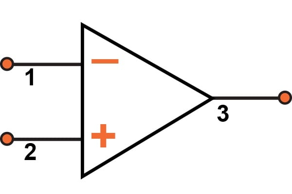
Fig 1.1 Op-amp symbol
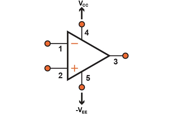
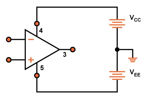
Fig 1.2 Op-amp connections to the dc power supplies
Besides the five terminals discussed thus far, an op-amp may have other terminals for specific purposes. Such purposes might be for frequency compensation and negative feedback or offset nulling, which reduces small DC offsets that can be amplified.
Introducing Characteristics of the Ideal Operational Amp
Looking at the actual functions of the circuit inside the op-amp, we see that it is designed to determine the difference between voltage signals that are applied directly to the two input terminals (the difference of v2 - v1). Once this quantity is found, it is then multiplied by a number A, and in turn, the voltage results in the term A(v2-v1). From here on out, when the voltage is referred to at the terminal, it is meant to be the voltage between that individual terminal and the ground; hence v1 is the voltage applied between terminal 1 and the ground.
An ideal op-amp shouldn't be drawing any current for the inputs; meaning, the current into terminal 1 and signal into terminal 2 are both zero. This is to say that the input impedance of an ideal op-amp is supposed to be infinite.
Focusing on the output terminal now, it should act as though it is a terminal of an ideal voltage source. Simply put, the voltage across terminal 3 and ground will always equate to A(v2 - v1), and independent of the current that may or may not be drawn from the third terminal into a load impedance.
With all of this stated, a model can be illustrated for the op-amp shown in Fig 1.3. Looking at the model, one can see that the output terminal has the same sign as v2 but opposite sign of v1. With this in mind, the input terminal is called the inverting input terminal, being denoted by a "-" sign while the input terminal 2 is called the noninverting input terminal and is denoted by a "+" sign.
As stated before, the op-amp is designed to sense a difference between voltage signals and will ignore any given signal that is common to both inputs. What this means, is that if v1 = v2 = 1 V, then the output will accordingly (ideal) be zero. This phenomenon is also known as what's called common-mode rejection. This can also be stated as zero common-mode gain, or analogously, infinite common-mode rejection. For now, we can say that the op-amp is a differential input, single-ended output amplifier, with the latter term pertaining to the fact that this op amp's output lies between the ground and terminal 3.
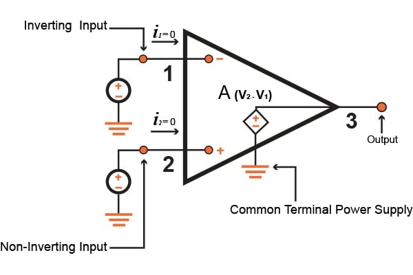
Figure 1.3 Circuit model of ideal op-amp
The term A, is what is known as the differential gain. It is known to be this because it is the desired gain of the op-amp when various signals are applied to the two inputs, 1 and 2. Another name that can we associated with the term is open-loop gain. This gain can be obtained when there is no feedback used in the IC op-amp. Normally, the open-loop gain tends to have an exceptionally high value; an ideal op-amp actually has an infinite open-loop gain.
One characteristic worth noting of op-amps are dc amplifiers or direct-coupled, which stands for dc or direct current since it amplifies signals with frequencies close to zero. Considering that op-amps are direct-coupled ICs, they are much more versatile which allows us to use them in many more important applications. However, direct-coupling can cause some serious problems that will be discussed later on.
Moving over to bandwidth, an ideal op-amp has gain A that will remain constant to a frequency of zero and all the way to an infinite frequency. In other words, an ideal amp can amplify signals of any frequency with an equal gain which allows them to have infinite bandwidth. Thus far, all characteristics and properties of ideal op-amps have been discussed, except one: the gain, A, of an ideal op-amp should have a value that is large and infinite, ideally speaking. However, this brings a good question: if there is a gain of an infinite value, how can the op-amp be used in any application? This can be answered rather simply because the op-amp will not be used solely in an open-loop configuration in almost every application one could think of. In the following article, I will discuss how other components will come into play by applying a feedback to complete or close the loop around the op-amp.
Summary
As of now, we have discussed how an operational amplifier is so popular due to its versatility, as well as the characteristics and functions of the ideal op-amp. To summarize, the characteristics of an ideal op-amp are as follows:
- Infinite bandwidth due to the ideal gain inside of the op-amp
- Infinite open-loop gain A
- Infinite or zero common-mode gain
- Input impedance of an infinite value
- Output impedance of zero
You should now know what an op-amp is used for as well as what to look for in an ideal op-amp. In a forthcoming article, we will pick up where we left off; we will introduce and explain the two different types of voltage gain as well as the inverting configuration of an op-amp that is used for inverting a signal input to have an inverted output gain. We will also go further into the closed-loop gain and how op-amps are not used alone rather with components. Finally, the article will talk about the analysis of the inverting configuration of the op-amp and the effects of having a finite open-loop gain. If you have any questions or comments, please leave them below!
Next Article in Series: The Inverting Configuration of an Amplifier


Am interested in analog computing, particularly signed addition. I have an xfer function requirement that, for now, is done in two parts according to algebraic signs of arguments, then analog switches to steer the result according to a comparator on one of the args. Want to replace all this with a single unified signed addition transfer function. Maybe a non-inverting summing amp for starters, with zero established somewhere between supply rails. Intuitively, a separate 2-resister divider with “zero” taken between them and applied at the away-end of the v-divider feedback resistor net (sets gain at the inverting junction) where we usually see Vee, V-, or Ground?