Facebook
 Google
 GitHub
 Linkedin
Understanding Varactor and PLL-Based FM Generation Using Crystal Oscillators
In this article, we examine two different methods of producing wideband FM signals. Both use crystal oscillators to provide improved frequency stability.
Over the years, many different circuits have been developed to generate FM signals. In previous articles, we learned how reactance modulators and varactor diodes are employed to make LC oscillators tunable for direct FM generation. This article explains how a varactor diode can be used with a crystal oscillator to create a voltage-controlled oscillator (VCO) for generating direct FM waves. Toward the end of the article, we'll briefly explain the PLL-based method of FM generation, which also uses a crystal oscillator.
Direct FM Generation Using LC Oscillators
Before we jump in, let's briefly review the varactor-LC oscillator combination. Figure 1 shows how a varactor in parallel with an oscillator's resonant circuit can be incorporated to generate direct FM waves.
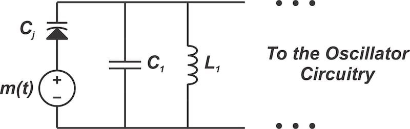
Figure 1. Using a varactor to adjust the resonant frequency of a tuned circuit. Image used courtesy of Steve Arar
Figure 2 provides further details on connecting the varactor to the LC oscillator.
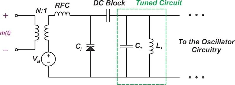
Figure 2. Connecting a varactor to an oscillator for FM generation. Image used courtesy of Steve Arar
The modulating signal, m(t), is superimposed onto a DC bias voltage (VB) via a transformer. The resulting voltage appears across the varactor. The RF choke separates the low-frequency section of the circuit from the high-frequency section. Finally, the DC block capacitor ensures that the varactor's DC bias voltage doesn't impact the oscillator circuitry.
The main drawback of this type of circuit is that the carrier frequency tends to drift, requiring complex feedback circuitry for center frequency stabilization. An alternative method for achieving a stable carrier frequency involves combining a varactor with a crystal oscillator, as we'll discuss below.
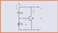
FM Generation Using the Varactor-Crystal Combination
In a crystal oscillator, a varactor can be placed in series or in parallel with the crystal to create a variable-frequency oscillator. Figure 3 shows a simplified diagram of a crystal oscillator with a parallel varactor.
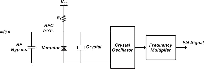
Figure 3. The varactor-crystal combination provides enhanced center frequency stability. Image used courtesy of Steve Arar
The crystal provides a stable carrier frequency; the varactor's variable capacitance pulls the crystal's frequency slightly away from its natural resonance. Applying the message signal to the varactor means that the output frequency changes in response to the message, creating an FM wave. Note that the separation between the crystal's series and parallel resonant frequencies must be sufficient to avoid oscillation at the wrong frequency.
The main idea here is to let the crystal provide a stable carrier frequency and use the varactor's variable capacitance to directly generate an FM wave. The downside, however, is that the crystal establishes the oscillation frequency so firmly that the varactor's capacitance changes lead to only slight variations in the output frequency. Adding a capacitor in parallel with the crystal might cause the frequency to shift by several tens to several hundreds of ppm.
For example, assume that we achieve a deviation of ±500 Hz around a 5 MHz center frequency. In this case, a 100-fold frequency multiplication produces a frequency deviation of ±50 kHz around 500 MHz. However, a reactance modulator operating at 5 MHz might have a frequency deviation of ±4 kHz. By applying a ×18 frequency multiplication, we achieve an output deviation of 4 kHz × 18 = 72 kHz, which is close to that required for commercial FM applications.
In short, the crystal oscillator provides a stable carrier frequency but requires a larger frequency multiplication factor. With the LC oscillator, it's the other way around. While it can't provide a sufficiently stable carrier, it can generally achieve the desired frequency deviation with minimal frequency multiplication.
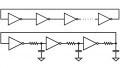
Assessing the Pullability of a Crystal
To determine the extent to which the frequency of a crystal will shift when adjusting the parallel capacitor (its 'pullability'), we need the crystal's circuit model parameters. Alternatively, the manufacturer may provide a pulling curve like the one in Figure 4.
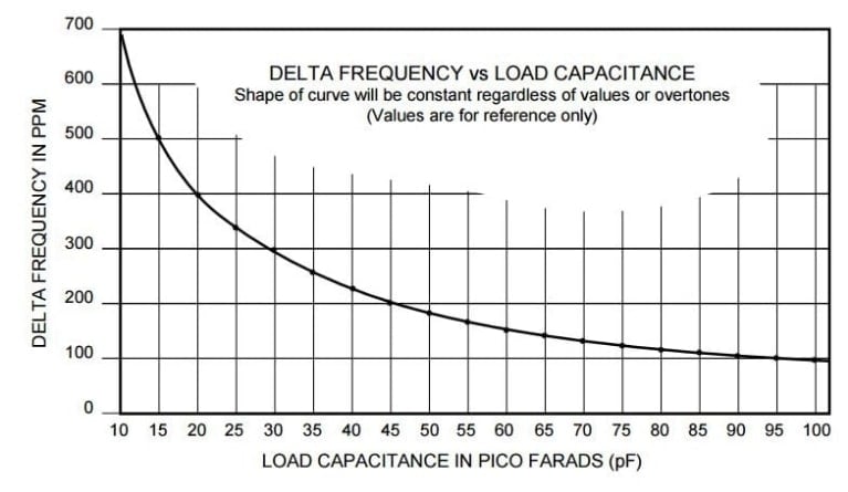
Figure 4. An example of a crystal pulling curve. Image used courtesy of Ecsxtal
Figure 4 is a fairly typical pulling curve. It shows that the frequency changes from +100 ppm to +700 ppm with respect to the series resonant frequency of the crystal as the crystal's load capacitance changes from 100 pF to 10 pF.
In addition to the pullability of the crystal, we also need to consider the linearity of the frequency variations. The frequency change may be linear only over a limited range of load capacitance variation, such as up to a change of 10 ppm. The frequency deviation achieved is quite small.
Connecting the Varactor to the Crystal
Figure 5 provides further details on connecting the varactor to the crystal oscillator.
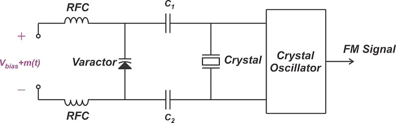
Figure 5. Using capacitive coupling to connect the varactor to the crystal oscillator. Image used courtesy of Steve Arar
The message signal is applied to the varactor through two RF chokes. Capacitors C1 and C2 are used to connect the varactor to the crystal. These capacitors are significantly smaller than the varactor and help prevent the varactor from excessively loading the crystal. However, the presence of C1 and C2 influences the effective capacitance change that the crystal undergoes for a specific capacitance change in the varactor.
To understand this, consider the simplified circuit model in Figure 6.
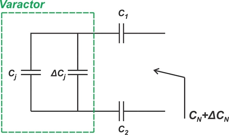
Figure 6. Simplified model of the crystal's load network. Image used courtesy of Steve Arar
In this model, Cj represents the center value of the varactor's capacitance. ΔCj denotes its variations. The total load capacitance presented by this network can be viewed as comprising a central capacitance value (CN) plus a variation (ΔCN) caused by ΔCj.
To assess the impact of the load network on the crystal oscillator, we need to calculate the ratio of ΔCN to CN. If we represent the capacitance of the series combination of C1 and C2 as C12, we can express the total load capacitance as:
$$C_{N} ~+~ \Delta C_{N} ~=~ \frac{C_{12} ~\times~ \big (C_{j}~+~ \Delta C_{j} \big )}{C_{12} ~+~ \big (C_{j}~+~ \Delta C_{j} \big )}$$
Equation 1.
Factoring out the constant terms from the numerator and denominator, we obtain:
$$C_{N} ~+~ \Delta C_{N} ~=~ \frac{C_{12}C_{j}}{ C_{12} ~+~ C_{j} } \times \frac{ 1~+~ \frac{\Delta C_{j}}{C_{j}} }{ 1~+~ \frac{\Delta C_{j}}{C_{12} ~+~ C_{j}} }$$
Equation 2.
Assuming that ΔCj is much smaller than C12 + Cj, we can simplify the above expression using the following approximation:
$$\frac{1}{1~+~x} ~\approx~ 1~-~x \quad \text{for} \quad x ~\ll~ 1$$
Equation 3.
Hence, Equation 2 can be approximated as:
$$C_{N} ~+~ \Delta C_{N} ~\approx~ \frac{C_{12}C_{j}}{ C_{12} ~+~ C_{j} } ~\times~ \big ( 1~+~ \frac{\Delta C_{j}}{C_{j}} \big ) ~\times~ \big ( 1 ~-~ \frac{\Delta C_{j}}{C_{12} ~+~ C_{j}} \big )$$
Equation 4.
Using basic algebra, this equation yields:
$$C_{N} ~+~ \Delta C_{N} ~\approx~ \frac{C_{12}C_{j}}{ C_{12} ~+~ C_{j} } ~\times~ \Big ( 1~+~ \frac{\Delta C_{j}}{C_{j}} ~-~ \frac{\Delta C_{j}}{C_{12} ~+~ C_{j}} ~-~ \frac{\Delta C_{j} ~\times~\Delta C_{j}}{C_{j} \big ( C_{12} ~+~ C_{j} \big )} \Big )$$
Equation 5.
As the last term involves squaring a small value, it can be considered negligible relative to the other terms. After excluding this negligible term, algebraic calculations yield the total capacitance as:
$$C_{N} ~+~ \Delta C_{N} ~\approx~ \frac{C_{12}C_{j}}{ C_{12} ~+~ C_{j} } ~\times~ \Big ( 1~+~ \frac{\Delta C_{j} ~\times~ C_{12}}{C_{j} \big (C_{12} ~+~ C_{j})} \Big )$$
Equation 6.
Finally, the ratio of ΔCN to CN is obtained as:
$$\frac{\Delta C_{N}}{C_{N}} ~\approx~ \frac{\Delta C_{j} ~\times~ C_{12}}{C_{j} \big (C_{12} ~+~ C_{j})} ~\approx~ \frac{\Delta C_{j}}{C_j} ~\times~ \frac{C_{12}}{C_{j}}$$
Equation 7.
An important implication of Equation 7 is that the fractional change in the crystal's load capacitance (ΔCN/CN) is smaller than the fractional change in the varactor capacitance (ΔCj/Cj). It's reduced by the ratio C12/Cj. For instance, if Cj = 10C12, then C12/Cj = 1/10 and the fractional capacitance change across the crystal is one-tenth that produced by the varactor.
To find the frequency deviation of the varactor-crystal oscillator combination, one can use a procedure similar to the one described above and a circuit model of the crystal. However, due to space constraints, this analysis won't be covered here. Interested readers can refer to the classic RF design book "Solid State Radio Engineering" by Charles W. Bostian, Frederick H. Raab, and Herbert L. Krauss for a summary of the analysis.
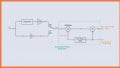
FM and PM Generation With a Phase-Locked Loop
Another way to generate wideband FM signals is to incorporate a VCO into a phase-locked loop (PLL) arrangement. As Figure 7 illustrates, this method also works to produce phase-modulated (PM) waves.

Figure 7. Incorporating a VCO into a PLL arrangement to generate wideband PM waves. Image used courtesy of Steve Arar
Here, the VCO frequency is greater than the crystal oscillator frequency (fosc) by a factor of N. The PLL locks to the stable frequency source provided by the crystal oscillator. This sets the center frequency (fc) of the output FM wave. The tolerance of the output carrier frequency is determined by the crystal oscillator circuit.
The message signal, m(t), is introduced into the loop as an error signal after the lowpass filter. This prompts the loop to adjust the VCO and create the message-dependent phase shift between its output and the reference signal.
In the steady state, the output phase is proportional to the modulating signal. The above configuration therefore serves as a phase modulator. We produce the corresponding FM wave by applying the integral of the modulating signal to the system (Figure 8).
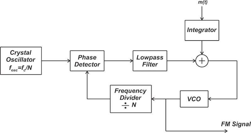
Figure 8. Incorporating a VCO into a PLL arrangement to generate wideband FM waves. Image used courtesy of Steve Arar
Note that the PLL's bandwidth should exceed the modulating signal's bandwidth to prevent the loop from distorting the signal. The linear operating range of this type of modulator depends primarily upon the phase detector.
There exists another PLL-based FM generator that employs a narrowband FM signal as one of the inputs to the phase detector. This modulator is not covered here, but you can find more information in the book "Electronic Communications: A Systems Approach" by J. S. Beasley and others.
Wrapping Up
A direct FM generator with a non-crystal oscillator achieves the desired frequency deviation with minimal frequency multiplication. However, it lacks sufficient carrier frequency stability. By contrast, the varactor-crystal combination offers a stable carrier frequency but necessitates a higher frequency multiplication factor.
When using the varactor-crystal arrangement, we need to account for the effect of the coupling capacitors placed between the varactor and the crystal. Wideband angle-modulated signals can also be generated by injecting the message signal into a PLL arrangement.
This article is Part 5 of a seven-part series on FM signal generation. All articles in this series are listed below in order of publication:
- Introduction to Reactance Modulators for Generating FM Signals
- An FM Generator Circuit Using the Capacitance of a Collector-Base Junction
- Using Varactor Diodes for FM Signal Generation
- Improving the Frequency Deviation and Stability of a Direct FM Generator
- Understanding Varactor and PLL-Based FM Generation Using Crystal Oscillators
- Armstrong's Method of FM Generation
- FM Generation Techniques: Solved Examples
Related Content