Facebook
 Google
 GitHub
 Linkedin
An FM Generator Circuit Using the Capacitance of a Collector-Base Junction
In this article, we examine a reactance modulator design that employs the variable capacitance of a bipolar junction transistor to modulate the output of a Colpitts oscillator.
In direct FM generation, the modulating signal directly alters the frequency of a carrier oscillator. To accomplish this, we need an LC oscillator with an adjustable capacitance or inductance. In the previous article, we learned how combining a transistor with an RC feedback path can produce a tunable reactance suitable for direct FM transmitters. In this article, we'll delve into another method of creating a tunable capacitor for direct FM generation.
This method leverages the fact that the collector-base junctions of BJT transistors are typically reverse-biased. A reverse-biased junction has a capacitance that varies with the bias voltage. As we'll see, this allows it to be used as a reactance modulator.
Two Types of Reactance Modulator
Figure 1 shows a simplified schematic of the reactance modulator from the preceding article.

Figure 1. A reactance modulator producing a tunable capacitance. Image used courtesy of Steve Arar
When viewed from the collector-emitter terminals, Figure 1 produces an equivalent capacitance of Ceq = gmR1C1. The circuit incorporates the external feedback path formed by R1 and C1 to create a tunable reactance.
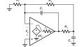
It's also possible to construct a voltage-controlled capacitor by using the reverse-biased collector-base junction of a BJT. Figure 2 shows a Colpitts oscillator that uses this technique.

Figure 2. A tunable Colpitts oscillator that uses the collector-base junction capacitance. Image used courtesy of Steve Arar
Though the circuits in Figure 1 and Figure 2 are both referred to as reactance modulators, they operate on entirely different principles. In Figure 2, the collector-base capacitance (Cμ) is used as a variable capacitance. Note that Cμ is actually part of the transistor (Q1), not an external capacitor.
Additionally, note that swapping the positions of R1 and C1 in Figure 1 results in the circuit producing a tunable inductive reactance. Because the circuit in Figure 2 uses the transistor's variable junction capacitance, it can't generate a tunable inductance.
We'll return to Figure 2 later on in the article. Before we do so, let's make sure we understand the key features of Cμ.
The Collector-Base Junction Capacitance
Measurements show that the variation of Cμ with the voltage across the junction for most devices can be approximated by:
$$C_{\mu} ~=~ \frac{C_{\mu 0}}{\big ( 1 ~-~ \frac{V_D}{V_0} \big )^n}$$
Equation 1.
where:
VD is the forward bias on the junction
Cμ0 is the junction capacitance for VD = 0
V0 denotes the built-in potential of the junction (zero applied bias)
n is an exponent that depends on the doping profile of the PN junction.
For linearly graded junctions, n = 1/3; this value becomes n = 1/2 for abrupt junctions. Hyper-abrupt junctions produce exponent values greater than 1/2. For a given voltage range, the capacitance variation range increases in the following order:
- Linearly graded junctions.
- Abrupt junctions.
- Hyper-abrupt junctions.
The above equation is not valid when VD approaches V0. For VD greater than about V0/2, a more accurate analysis shows that the junction capacitance is somewhat different from that predicted by the above equation. Figure 3 contrasts the results from both analyses. Note that this image uses ψ0 in place of V0.

Figure 3. The variation of the reverse-biased junction capacitance with the forward bias (ψ0). Image used courtesy of Paul R. Gray
To better understand the variation of Cμ with the bias voltage, let's consider an example.
Example 1: Determining the Collector-Base Capacitance of a BJT Transistor
For an NPN transistor, we have Cμ0 = 10 fF, n = 0.3, and V0 = 0.5 V. Let's find Cμ when the collector-base voltage (VCB) changes from 1 V to 3 V.
Applying Equation 1 for VCB = 1, we obtain:
$$C_{\mu} ~=~ \frac{C_{\mu 0}}{\big ( 1 ~-~ \frac{V_D}{V_0} \big )^n} ~=~ \frac{10 \ \text{fF}}{\big ( 1 ~-~ \frac{-1}{0.5} \big )^{0.3}} ~=~7.19 \ \text{fF}$$
Equation 2.
Note that VD is the forward voltage across the junction. In our example, the collector-base voltage is VCB = 1 V, so the forward voltage applied to the junction is –1 V. For VCB = 3 V, we have:
$$C_{\mu} ~=~ \frac{C_{\mu 0}}{\big ( 1 ~-~ \frac{V_D}{V_0} \big )^n} ~=~ \frac{10 \ \text{fF}}{\big ( 1 ~-~ \frac{-3}{0.5} \big )^{0.3}} ~=~5.58 \ \text{fF}$$
Equation 3.
The above example shows that increasing the reverse bias voltage decreases the junction capacitance, but why does this happen? The increase in reverse bias voltage increases the electric field across the junction, which in turn widens the depletion region. A wider depletion region means that the effective distance between the "plates" of the capacitor (the P-type and N-type regions) is larger, leading to a decrease in capacitance.
Estimating Cμ Under Large Reverse Bias Conditions
When the applied reverse bias voltage is much greater than the built-in potential (VD ≫ V0), we can simplify Equation 1 as follows:
$$C_{\mu} ~=~ \frac{C_{\mu 0}}{\big ( 1 ~-~ \frac{V_D}{V_0} \big )^n} ~\approx~ \frac{C_{\mu 0}}{\big ( - \frac{V_D}{V_0} \big )^n} ~=~ \frac{C_{\mu 0} V_0^n}{\big ( - V_{D} \big )^n} ~=~ \frac{A}{\big ( - V_{D} \big )^n}$$
Equation 4.
where A = Cμ0V0n and is a constant.
Now that we've cemented our understanding of the junction capacitance, we're ready to analyze the Colpitts oscillator in Figure 2.
Analyzing the Colpitts Oscillator With Tunable Collector-Base Capacitance
Looking back at Figure 2, we see that Cμ appears in parallel with the LC circuit of the oscillator. The total capacitance in the tuned LC circuit is:
$$C_{tot} ~=~ \frac{C_{1} C_{2}}{C_1 ~+~ C_2} ~+~ C_{\mu}$$
Equation 5.
Assuming that the exponent associated with the collector-base junction is n = 0.5, Equation 4 yields Cμ as:
$$C_{\mu} ~=~ \frac{A}{\sqrt{- V_{D}}}$$
Equation 6.
The forward voltage across the base-collector junction is:
$$V_{D} ~=~ V_{BC} ~=~ v_m(t) ~-~ V_{CC}$$
Equation 7.
where vm(t) represents the message signal applied to the base of the transistor. Combining Equations 6 and 7, we have:
$$C_{\mu} ~=~ \frac{A}{\sqrt{V_{CC}~-~v_m(t) }} ~=~ \frac{A}{\sqrt{V_{CC}}} ~\times~ \frac{1}{\sqrt{1~-~ \frac{v_m(t)}{V_{CC}}}}$$
Equation 8.
Assuming that vm(t) is much less than VCC, we can simplify the above expression using the following approximation:
$$\frac{1}{\sqrt{1~-~x}} ~\approx~ 1~+~\frac{x}{2} \quad for \quad x ~\ll~1$$
Equation 9.
Thus, Cμ can be approximated as:
$$C_{\mu} ~\approx~ \frac{A}{\sqrt{V_{CC}}} ~\times~ \big ( 1~+~ \frac{v_m(t)}{2V_{CC}} \big ) ~=~ C_{0} ~\times~\big ( 1~+~k v_m(t) \big )$$
Equation 10.
where k is a proportionality constant. Therefore, the collector-base capacitance is approximated by a constant value (C0) plus a term that's proportional to the message signal. Combining Equations 5 and 10, the total capacitance is obtained as:
$$\begin{eqnarray} C_{tot} &~=~& \frac{C_{1} C_{2}}{C_1 ~+~ C_2} ~+~ C_{\mu} ~=~ \underbrace{\frac{C_{1} C_{2}}{C_1 ~+~ C_2} ~+~ C_{0} }_{C_k}~+~ \underbrace{C_{0}k}_{k_1} ~\times~ v_m(t) \\ &~=~& C_{k} ~+~ k_{1} v_m(t) \end{eqnarray}$$
Equation 11.
where:
Ck is the center value of the capacitance in the oscillator's tuned LC circuit
k1 is a proportionality constant that determines the capacitance variation caused by the message signal.
Having the total capacitance (Ctot), we can now determine the instantaneous frequency of oscillation:
$$f_i ~=~ \frac{1}{2 \pi \sqrt{L_{1}C_{tot}}} ~=~\frac{1}{2 \pi \sqrt{L_{1} \big ( C_k ~+~ k_1 v_m(t) \big )}}$$
Equation 12.
Finally, let's assume that the time-dependent part of the capacitance is much less than its constant part. We then apply the approximation in Equation 9 to Equation 12. This leads to:
$$f_i ~=~ \underbrace{\frac{1}{2 \pi \sqrt{L_{1} C_{k}}}}_{f_k} ~\times~ \frac{1}{{ \sqrt{1 ~+~ \frac{k_1}{C_k} v_m(t) }}} ~\approx~ f_{k} ~\times~ \big ( 1~-~ \frac{k_1}{2C_k} v_m(t) \big )$$
Equation 13.
where fk denotes the constant part (or the center value) of the oscillation frequency, and the second term shows that the message signal linearly changes the instantaneous oscillation frequency. We can now determine the frequency deviation normalized to fk as follows:
$$\frac{|\Delta f|}{f_k} ~\approx~ \frac{k_1}{2C_k} v_m(t) ~=~ \frac{C_0 }{4C_k V_{CC}} v_m(t) ~=~ \frac{A}{4C_k \sqrt{V_{CC}^3}} v_m(t)$$
Equation 14.
In Equation 14, Equations 10 and 11 are used to express k1 in terms of A and VCC. To calculate the maximum frequency deviation, we must use the maximum of vm(t) in this equation.
Example 2: Determining the Frequency Deviation of the Colpitts Oscillator
Assume that the Colpitts oscillator of Figure 2 uses:
- VCC = 5 V
- L1 = 10 μH
- C1 = 102 pF
- C2 = 0.02 μF.
The collector-base junction's parameters are:
- Cμ0 = 5 PF
- V0 = 0.5 V
- n = 0.5.
Let's determine the frequency deviation of the oscillator for a sinusoidal message signal of unity amplitude.
To solve this problem, we'll apply Equation 14. Before that, however, we need to calculate the parameters used in this equation. We first use Equation 4 to find the constant A:
$$A ~=~ C_{\mu 0} V_0^n ~=~ 5 ~\times~ 0.5^{0.5} ~=~ 3.53$$
Equation 15.
From Equation 10, the constant part of the collector-base capacitance is:
$$C_0 ~=~ \frac{A}{\sqrt{V_{CC}}} ~=~ \frac{3.53}{\sqrt{5}}~=~ 1.58 \ \text{pF}$$
Equation 16.
According to Equation 11, the constant part of the capacitance in the resonant circuit is:
$$C_{k} ~=~ \frac{C_{1} C_{2}}{C_1 ~+~ C_2} ~+~ C_{0}~=~\frac{102 ~\times~ 20000}{102~+~20000}~+~1.58~=~103 \ \text{pF}$$
Equation 17.
Using Equation 13, we obtain the center frequency of oscillation:
$$f_{k} ~=~ \frac{1}{2 \pi \sqrt{L_{1} C_{k}}} ~=~ \frac{1}{2 \pi \sqrt{10 ~\times~ 10^{-6} ~\times~ 103 ~\times~ 10^{-12}}} ~=~ 4.96 \ \text{MHz}$$
Equation 18.
Finally, substituting the values we obtained into Equation 14, we find the frequency deviation:
$$|\Delta f| ~\approx~ \frac{A}{4C_k \sqrt{V_{CC}^3}} ~\times~ f_{k} ~=~ \frac{3.53}{4 ~\times~ 103 ~\times~ \sqrt{5^3}} ~\times~ 4.96 \ \text{MHz} ~=~ 3.8 \ \text{kHz}$$
Equation 19.
Because the message signal is a sinusoidal wave with an amplitude of unity, vm(t) = 1 in the preceding calculation.
A Tunable Oscillator Using the Transistor's Collector-Base Junction Capacitance
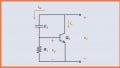
Figure 4 illustrates a tunable oscillator created by connecting the Cμ-based reactance modulator to the resonant circuit of a Colpitts oscillator.

Figure 4. A Cμ-based reactance modulator connected to a Colpitts oscillator. Image used courtesy of Steve Arar
Q1's collector-base capacitance functions as a variable capacitance. The capacitance is a function of the modulating signal, which is applied to Q1's base through the resistor R1.
At the oscillation frequency, capacitor C1 behaves like a short circuit, connecting the reactance modulator's output to the oscillator's tank circuit. Resistors R2 and R3 form a voltage divider network that provides bias to Q1. Resistor R4 provides emitter feedback to thermally stabilize Q1.
In the Colpitts oscillator, Q2 serves as the amplifying device. The resonant tank circuit is composed of inductor L1 and capacitors C3 and C4. Capacitor C2 delivers the necessary positive feedback to initiate and sustain oscillation.
The message signal causes a change in the capacitance observed at the collector of Q1. When the message signal increases, the effective capacitance at Q1's collector increases. Consequently, the oscillation frequency decreases (see Equations 10 and 13). When the message signal decreases, the collector-base capacitance decreases and the oscillation frequency increases.
Wrapping Up
In this article, we created a voltage-controlled capacitor by using the collector-base junction of a BJT transistor, which is typically reverse-biased. For a reverse-biased junction, increasing the reverse bias voltage decreases the junction capacitance. This variable capacitance can be connected to the resonant circuit of an oscillator to construct a tunable oscillator suitable for direct FM generation.
This article is Part 2 of a seven-part series on FM signal generation. All articles in this series are listed below in order of publication:
- Introduction to Reactance Modulators for Generating FM Signals
- An FM Generator Circuit Using the Capacitance of a Collector-Base Junction
- Using Varactor Diodes for FM Signal Generation
- Improving the Frequency Deviation and Stability of a Direct FM Generator
- Understanding Varactor and PLL-Based FM Generation Using Crystal Oscillators
- Armstrong's Method of FM Generation
- FM Generation Techniques: Solved Examples
Related Content