Facebook
 Google
 GitHub
 Linkedin
Volume
Designing Analog Chips
Chapter
Simulation
SPICE Simulation of Bond Pads and Package Pins
If you're working at high frequencies—say, above 50 MHz—you need to consider the properties of the pads, the ESD protection devices, the bonding wires, and the package pins (Figure 3-17).
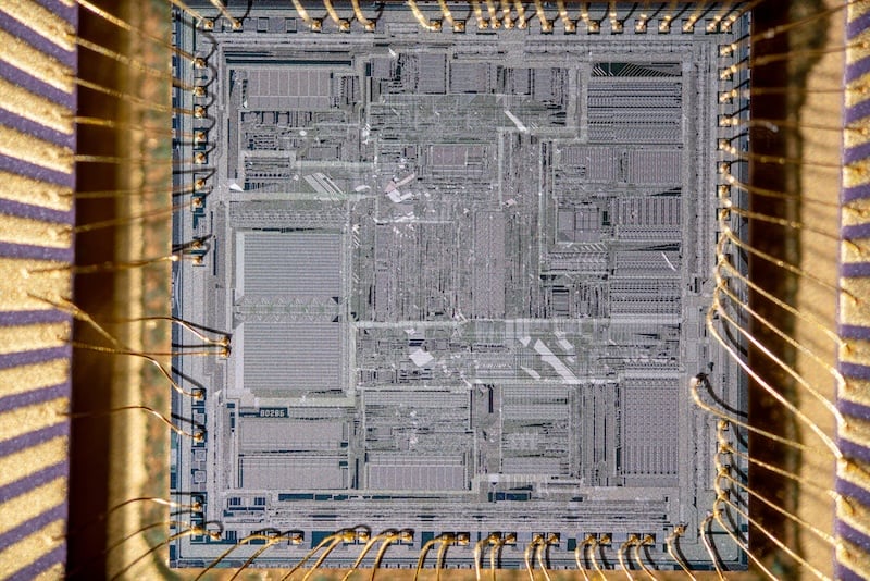
Figure 3-17. Magnified view of IC showing bond wires connecting pads to leadframe pins. Image used courtesy of Adobe Stock
A pad has a capacitance to the underlying layer (usually ground). With an ESD protection device, this can easily amount to more than 1 pF.
The bonding wire has an inductance. It may be small (perhaps 7 nH), but this depends on the length of the wire. The bonding wire inductance begins to play a role above about 100 MHz.
Then there's the package pin capacitance, which is not to ground. Rather, it's between pins. The value of this capacitance is typically about 1 pF, though its greatly dependent on the package.