Facebook
 Google
 GitHub
 Linkedin
DC Analysis in SPICE
To discuss DC analysis, let's use a simple example. Figure 3-1 shows a buffer—a very simple circuit with a voltage gain of one.
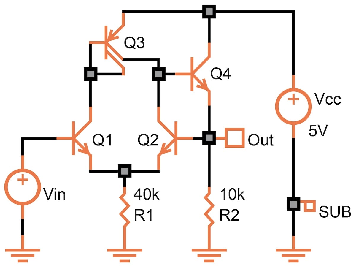
Figure 3-1. A simple example of a bipolar buffer for simulation. [click to enlarge]
The NPN transistors Q1 and Q2 form a differential stage. Q3 is a current mirror; Q4 is an emitter follower (more about this in the next two chapters). For the current mirror, we use a lateral PNP transistor with a split collector.
In the most basic DC analysis, we continuously change (sweep) Vin from 0 to 5 V and observe the output (Figure 3-2). The simulator tells us that the output follows the input, but only within the common-mode range: above about 0.6 V and below 4.1 V.
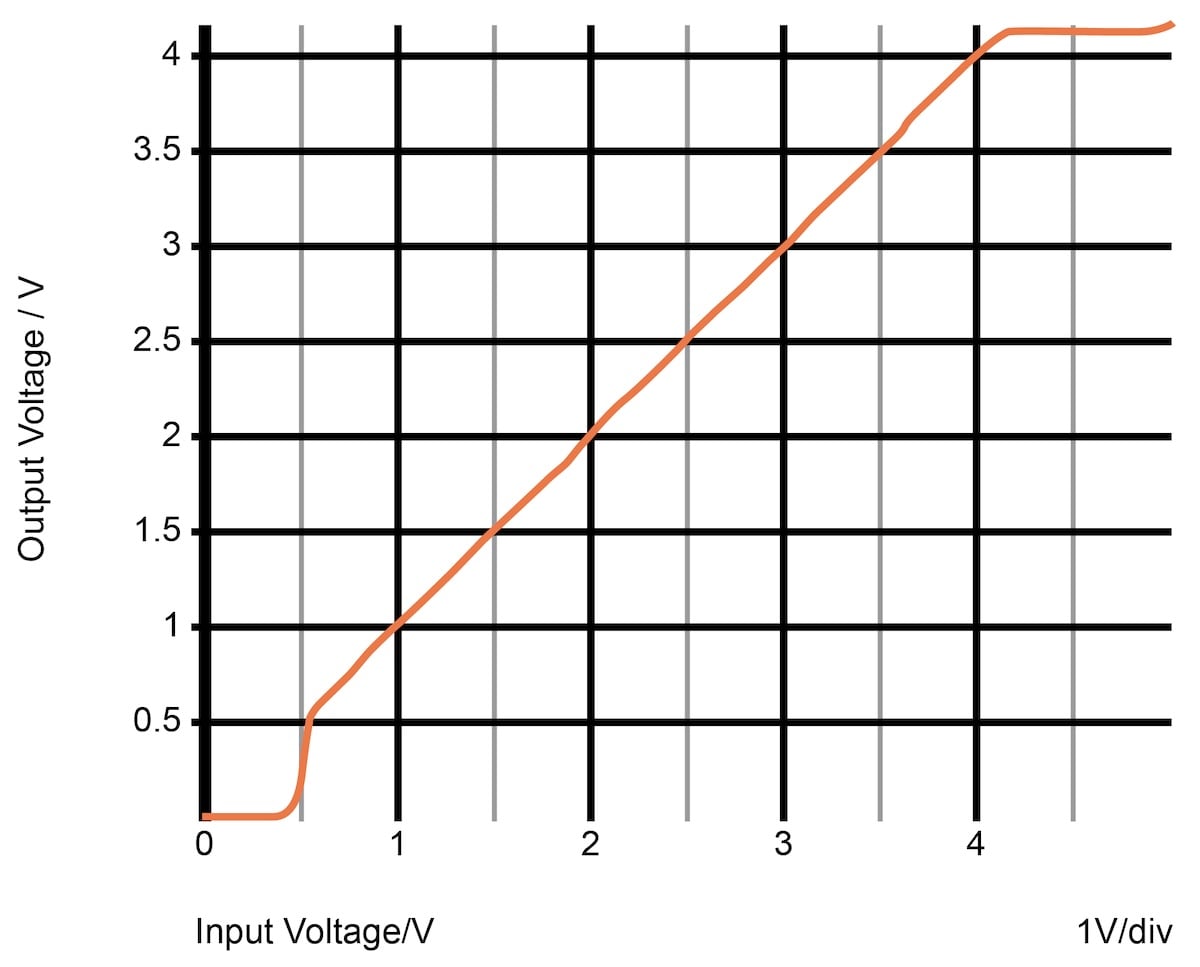
Figure 3-2. DC analysis of the bipolar buffer circuit showing the common-mode range. [click to enlarge]
You can enhance this analysis by repeating it at various temperatures. This can be done automatically by "stepping" the temperature, either at regular intervals or at three or four user-defined points.
While doing this, you can measure any of the following:
- The input current (either at the base of Q1 or at either terminal of Vin).
- The current consumption (at one of the terminals of Vcc).
- The substrate current (out of the symbol SUB).
- The power dissipation of the entire circuit or any component.
By placing a current source from the output node to ground, you can find the output impedance, thus determining how well the circuit handles a load.
There are two additional subcategories of DC analysis:
- Transfer function analysis gives you the relationship between two nodes. This isn’t used very often.
- Sensitivity analysis tells you which parameters (including transistor parameters) are most responsible for a change in a particular voltage or current at any node.