Facebook
 Google
 GitHub
 Linkedin
The Diode SPICE Model
As we saw in our discussion of diodes in semiconductor processes, no one junction in an IC should be used directly as a diode. A diode-connected transistor does this job with greater accuracy and far fewer side effects.
However, a bipolar transistor consists of at least two junctions. The junction diode is a fundamental element in the SPICE model file, even for a CMOS process. Figure 3-12 shows a simple diode model.
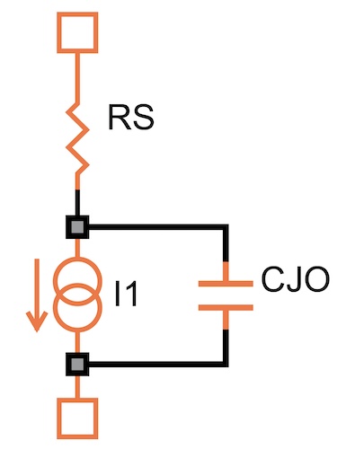
Figure 3-12. A simple diode equivalent circuit.
The model file is always in ASCII. In it, you might see the following statement:
.MODEL Diode1 D IS=1E-17 RS=20 CJO=0.85E-12
A model statement always starts with a dot. Next is the name of the device, which can be anything you want. In this case, it’s "Diode1." After the device name, the “D” says the device is a diode. The remaining entries are device parameters in amperes, ohms, and farads.
This is about as simple a diode model as you can possibly make it. Just three parameters are specified: IS, RS, and CJ0. Together, the diffusion current (IS) and the series resistance (RS) determine the DC characteristics; CJ0 specifies the junction capacitance. Let's start by looking at the DC behavior.
As we saw in the Analog Devices chapter, the current/voltage relationship of an ideal junction is given by:
$$I_1 ~=~ I_S \,\, e ^{ (\frac{qV_d}{ kT})}$$
where:
IS = the diffusion current
Vd = the voltage across the diode current source. This does not include the voltage drop across RS.
q = the electron charge
k = the Boltzmann constant
T = the temperature in Kelvin
In SPICE this diode equation is greatly expanded:
$$I_1 ~=~ I_S {\Bigg(} e ^ \frac{qV_d}{kTN} {\Bigg)} ~\times~ e ^{((\Delta T - 1) \times \frac{qE_g}{kTN}) }~\times~ \Delta T\frac {XTI}{N} ~+~ ISR {\Bigg(} e^ \frac {qV_d} {kTN_{R}} {\Bigg)} ~\times~ {\Bigg(}{\Big(}1- \frac {V_d} {V_J}{\Big)}^2 ~+~ 0.005 ^\frac{M}{2}{\Bigg)}$$
where:
N = the forward emission coefficient. The SPICE default value is 1.
Eg = the energy gap. The value of Eg is different for different materials—you would set it to 0.69 for a Schottky diode, 0.67 for germanium, and 1.43 for gallium arsenide. SPICE uses Eg = 1.11, the value for silicon, by default.
XTI = the temperature coefficient of IS. The SPICE default value is 3.
ΔT = the quotient of operating (junction) temperature to room temperature. By default, SPICE sets this to 300 K (about 27 °C).
Though this equation might appear utterly complicated at first, it really isn’t. If you look at the portion of the equation to the left of the plus sign, you’ll see that it’s made of three terms multiplied together. The parameters that go into these terms are listed above.
With these three terms, you can shape the basic exponential curve to match what’s actually measured. If you don’t list the parameters in the model statement, SPICE will assume the default values.
The portion of the equation to the right of the plus sign adds a leakage current, which is a small current in excess of the reverse current predicted by the ideal diode equation. You can modify the shape of its curve with the constants NR, M, and VJ.
With the parameters we’ve specified, the model makes the breakdown voltage of the diode infinite. You can limit this with the parameter BV and three companions:
TBV1 (its first-order temperature coefficient)
TBV2 (second-order temperature coefficient)
IBV (the current at which breakdown is specified)
There’s also IKF, which splits the DC curve into two regions. In ICs, this parameter is very rarely used.
Series Resistance and Junction Capacitance
The series resistance, RS, which also influences the DC behavior, has first and second-order temperature coefficients, TRS1 and TRS2.
The junction capacitance shown in the model, CJ0 (or CJO) is measured at 0 V. Since its value at different voltages (forward or reverse) depends on the grading of the junction (abrupt, diffused, implanted, etc.), it too is modified by three constants: VJ, M, and FC. If you don’t specify these parameters in the model statement, the following default values are used:
VJ = 1
M = 0.5
FC = 0.5
For a voltage across the diode (not including RS) equal to or less than the product of FC and VJ, the formula for junction capacitance is:
$$C ~=~ C_{J0} ~\times~ {\Big(} 1 ~-~\frac{V_d}{V_J} {\Big)} ^ {-M}$$
If the voltage across the diode is greater than FC × VJ, the formula is:
$$C ~=~ C_{J0} ~\times~ {\Big(} 1~-~FC {\Big)}^{-(1+M)} ~\times~ {\Big(} 1 ~-~ FC ~\times~ {\Big(}1~+~M {\Big)} ~+~ M ~\times~ \frac {V_d} {V_J} {\Big)}$$
Noise Parameters
There are two noise sources in a diode: the resistor (RS) and the current (I1). Without any additional parameters, these are treated as white noise sources—in other words, it’s assumed that the noise from them is the same at any frequency.
To account for flicker noise (which increases at low frequency), two constants—KF and AF—are used. When current source noise is calculated, the following expression is added:
$$\frac{KF ~\times~ I_1 ^{AF}}{f}$$
For a more detailed look at noise, please see the Analog Measurements chapter.