Facebook
 Google
 GitHub
 Linkedin
DC Electric Circuits
Inductance
20 questions By Tony R. Kuphaldt
-
Question 16 of 20
Components soldered into printed circuit boards often possess “stray” inductance, also known as parasitic inductance. Observe this resistor, soldered in to a circuit board:
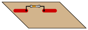
Where does the parasitic inductance come from? What is it about a resistor, mounted to a circuit board, that creates a (very) small amount of inductance? How is it possible to minimize this inductance, in case it is detrimental to the circuit’s operation?
Reveal answerInductance naturally exists along any conductor. The longer the conductor, the more inductance, all other factors being equal.
Notes:In high-frequency AC circuits, such as computer circuits where pulses of voltage oscillate at millions of cycles per second, even short lengths of wire or traces on a circuit board may present substantial trouble by virtue of their stray inductance. Some of this parasitic inductance may be reduced by proper circuit board assembly, some of it by a re-design of component layout on the circuit board.
According to an article in IEEE Spectrum magazine (”Putting Passives In Their Place”, July 2003, Volume 40, Number 7, page 29), the transient currents created by fast-switching logic circuits can be as high as 500 amps/ns, which is a [di/dt] rate of 500 billion amps per second!! At these levels, even a few picohenrys of parasitic inductance along component leads and circuit board traces will result in significant voltage drops.
-
Question 17 of 20
Many precision resistors utilize a wire-wound construction, where the resistance is determined by the type and length of wire wrapped around a spool. This form of construction allows for high precision of resistance, with low temperature sensitivity if certain metal alloys are used for the wire.
Unfortunately, though, wrapping wire around a spool forms a coil, which will naturally possess a significant amount of inductance. This is generally undesirable, as we would like to have resistors possessing only resistance, with no “parasitic” properties.
There is, however, a special way in which a wire coil may be wound so as to have almost no inductance. This method is called bifilar winding, and it is common in wire-wound resistor construction. Describe how bifilar winding works, and why it eliminates parasitic inductance.
Reveal answerI won’t directly describe how a bifilar winding is made, but I’ll give you a hint. Compare the inductance of a straight piece of wire, versus one that is folded in half:
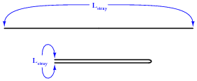
Now, how could a non-inductive coil of wire be made using the same principle?
Notes:This technique is very useful in reducing or eliminating parasitic inductance. Typically, parasitic inductance is not a problem unless very high rates of current change are involved, such as in high-frequency AC circuits (radio, high-speed digital logic, etc.). In such applications, knowing how to control stray inductance is very important to proper circuit operation.
-
Question 18 of 20
∫f(x) dx Calculus alert!
Digital logic circuits, which comprise the inner workings of computers, are essentially nothing more than arrays of switches made from semiconductor components called transistors. As switches, these circuits have but two states: on and off, which represent the binary states of 1 and 0, respectively.The faster these switch circuits are able to change state, the faster the computer can perform arithmetic and do all the other tasks computers do. To this end, computer engineers keep pushing the limits of transistor circuit design to achieve faster and faster switching rates.
This race for speed causes problems for the power supply circuitry of computers, though, because of the current “surges” (technically called transients) created in the conductors carrying power from the supply to the logic circuits. The faster these logic circuits change state, the greater the [di/dt] rates-of-change exist in the conductors carrying current to power them. Significant voltage drops can occur along the length of these conductors due to their parasitic inductance:

Suppose a logic gate circuit creates transient currents of 175 amps per nanosecond (175 A/ns) when switching from the “off” state to the ön” state. If the total inductance of the power supply conductors is 10 picohenrys (9.5 pH), and the power supply voltage is 5 volts DC, how much voltage remains at the power terminals of the logic gate during one of these “surges”?
Reveal answerVoltage remaining at logic gate terminals during current transient = 3.338 V
Notes:Students will likely marvel at the [di/dt] rate of 175 amps per nanosecond, which equates to 175 billion amps per second. Not only is this figure realistic, though, it is also low by some estimates (see IEEE Spectrum magazine, July 2003, Volume 40, Number 7, in the article “Putting Passives In Their Place”). Some of your students may be very skeptical of this figure, not willing to believe that ä computer power supply is capable of outputting 175 billion amps?!”
This last statement represents a very common error students commit, and it is based on a fundamental misunderstanding of [di/dt]. “175 billion amps per second” is not the same thing as “175 billion amps”. The latter is an absolute measure, while the former is a rate of change over time. It is the difference between saying “1500 miles per hour” and “1500 miles”. Just because a bullet travels at 1500 miles per hour does not mean it will travel 1500 miles! And just because a power supply is incapable of outputting 175 billion amps does not mean it cannot output a current that changes at a rate of 175 billion amps per second!