Facebook
 Google
 GitHub
 Linkedin
Discrete Semiconductor Devices and Circuits
JFET Amplifiers
15 questions By Tony R. Kuphaldt
-
Question 4 of 15
The simple JFET amplifier circuit shown here (built with surface-mount components) employs a biasing technique known as self-biasing:
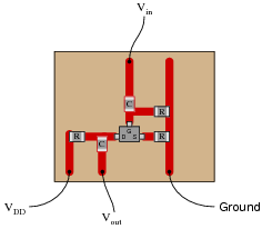
Self-biasing provides much greater Q-point stability than gate-biasing. Draw a schematic diagram of this circuit, and then explain how self-biasing works.
Reveal answer
Self-biasing uses the negative feedback created by a source resistor to establish a “natural” Q-point for the amplifier circuit, rather than having to supply an external voltage as is done with gate biasing.
Notes:The concept of negative feedback is extremely important in electronic circuits, but it is not easily grasped by all. Self-biasing of JFET transistors is a relatively easy-to-understand application of negative feedback, so be sure to take advantage of this opportunity to explore the concept with your students.
Ask your students to explain why Q-point stability is a desirable feature for mass-produced amplifier circuits, as well as circuits subject to component-level repair.
-
Question 5 of 15
The voltage gain for a “bypassed” common-emitter BJT amplifier circuit is as follows:

Common-source JFET amplifier circuits are very similar:

One of the problems with “bypassed” amplifier configurations such as the common-emitter and common-source is voltage gain variability. It is difficult to keep the voltage gain stable in either type of amplifier, due to changing factors within the transistors themselves which cannot be tightly controlled (r′e and gm, respectively). One solution to this dilemma is to “swamp” those uncontrollable factors by not bypassing the emitter (or source) resistor. The result is greater AV stability at the expense of AV magnitude:

Write the voltage gain equations for both “swamped” BJT and JFET amplifier configurations, and explain why they are similar to each other.
Reveal answer$$A_V \approx \frac{R_C}{R_E} \ \ \ \ \ \ \ \ \ \ Common-emitter \ \ BJT \ \ amplifier$$
$$A_V \approx \frac{R_D}{R_S} \ \ \ \ \ \ \ \ \ \ Common-source \ \ JFET \ \ amplifier$$
I’ll let you explain why these two voltage gain approximations share the same form. Hint: it has something to do with the magnitudes of the currents through each transistor terminal!
Follow-up question: explain mathematically why the emitter/source resistances succeed in “swamping” r′e and gm, respectively, in these more precise formulae. You should provide typical values for r′e and gm as part of your argument:
$$A_V=\frac{R_C}{R_E+r'_e} \ \ \ \ \ \ \ \ \ \ Common-emitter \ \ BJT \ \ amplifier$$
$$A_V=\frac{R_D}{R_S+\frac{1}{g_m}} \ \ \ \ \ \ \ \ \ \ Common-source \ \ JFET \ \ amplifier$$
Notes:Swamping is a common engineering practice, and one that students would do well to understand. It is unfortunate that parameters such as dynamic emitter resistance (r′e) and transconductance (gm) are so variable, but this does not have to be the end of the story. To be able to work around practical limitations such as these is the essence of engineering practice, in my opinion.
-
Question 6 of 15
The circuit shown here is a precision DC voltmeter:
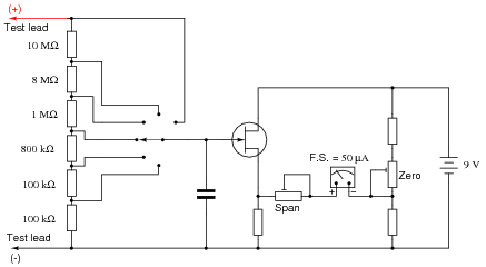
Explain why this circuit design requires the use of a field-effect transistor, and not a bipolar junction transistor (BJT).
Also, answer the following questions about the circuit:
- Explain, step by step, how an increasing input voltage between the test probes causes the meter movement to deflect further.
- If the most sensitive range of this voltmeter is 0.1 volts (full-scale), calculate the other range values, and label them on the schematic next to their respective switch positions.
- What type of JFET configuration is this (common-gate, common-source, or common-drain)?
- What purpose does the capacitor serve in this circuit?
- What detrimental effect would result from installing a capacitor that was too large?
- Estimate a reasonable value for the capacitor’s capacitance.
- Explain the functions of the “Zero” and “Span” calibration potentiometers.
Reveal answerThe voltage ranges for this meter are as follows:
- 0.1 volts
- 0.2 volts
- 1.0 volts
- 2.0 volts
- 10 volts
- 20 volts
The JFET is being used in the common drain configuration. A reasonable value for the capacitor would be 0.01 μF.
Notes:This relatively simple DC voltage amplifier circuit provides a wealth of educational value, both for understanding the function of the JFET, and also for review on past electrical/electronics concepts.
Note: John Markus’
Guidebook of Electronic Circuits, first edition, page 469, provided the inspiration for this circuit.