Facebook
 Google
 GitHub
 Linkedin
Discrete Semiconductor Devices and Circuits
Special Diodes
8 questions By Tony R. Kuphaldt
-
Question 4 of 8
The nonconducting depletion region of a PN junction forms a parasitic capacitance between the P and the N semiconductor region. Does the capacitance increase or decrease as a greater reverse-bias voltage is applied to the PN junction? Explain your answer.
Reveal answerThe junction capacitance will decrease as the reverse-bias voltage across the junction increases.
Challenge question: can you think of any practical applications for this variable-capacitance effect?
Notes:This question is a good review of capacitor theory, and also an opportunity to introduce a special kind of diode: the varactor.
-
Question 5 of 8
Explain what a Schottky diode is, and how it differs in construction and in function from a normal semiconductor PN junction diode.
Reveal answerA Schottky diode, otherwise known as a hot carrier diode, is formed by a junction of metal and N-type semiconducting material. These diodes have less forward voltage drop, faster reverse-recovery time, more reverse leakage current, and less reverse voltage capability than regular PN junction diodes.
Notes:Ask your students if they happened to research any datasheets for Schottky diodes, and if they have parameters to compare against typical PN junction rectifying diodes such as the 1N400x series.
-
Question 6 of 8
Draw the schematic symbol for a Schottky diode, and give some examples of typical applications for it.
Reveal answer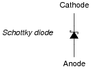
I’ll let you research some of the typical applications of Schottky diodes.
Notes:Ask your students to explain why the applications of Schottky diodes are well suited for these diodes’ unique capabilities. What is it about the typical applications that make use of these diodes’ fast reverse-recovery times and/or low forward voltage drop?
Note to your students that the schematic symbol for a Schottky diode is easily confused with the schematic symbol for a zener diode. Pay close attention to the symbol!