 Facebook
 Google
 GitHub
 Linkedin
Op Amp and Transistor-based Analog Square Wave Generator Design
Analog oscillator circuits are commonly used to create square wave clock signals for the timing of synchronous circuits. This article covers the theory, design, and key features of analog square wave generators.
Many electronic systems require a timing mechanism. This is most often done via a clock signal, which is a square wave of a specific frequency. For many applications, the clock signal is generated within the system via a square wave oscillator. However, this square wave signal can also be an input to the system.
Since many analog and digital circuits can be employed as square wave oscillators, we'll aim to cover both types; however, in this article, we will discuss the design of analog oscillators, cover their theory of operation, and review their advantages and disadvantages.
Op-amp Square Wave Generator Using an Astable Multivibrator
The first circuit we will study is a single op-amp circuit known as the astable multivibrator, as shown in Figure 1.
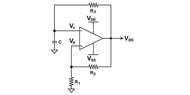
Figure 1. Single op-amp astable multivibrator oscillator for generating a square wave.
If you momentarily ignore the RC feedback from the output, VOUT, to the negative input, Vc, you might recognize the rest of this circuit as a Schmitt trigger with hysteresis. The Schmitt trigger has positive feedback and only two stable operating points (VOUT = VDD or VOUT = VSS). As we will explain, the astable multivibrator configuration relies on this positive feedback and hysteresis.
Upon startup of the circuit, we have a capacitor (C) completely discharged to the ground. Since there is an internal offset between the inputs of any amplifier, the positive feedback will ensure the output is driven to one of the two stable states (depending on whether the internal offset is positive or negative).
Now, let’s assume that VOUT is driven to the positive rail (VDD) at the start. At this point, Vc will begin to charge through the resistor, R3, and the voltage at Vp can be calculated using the resistor voltage divider equation:
$$ V_{p1} = V_{OUT}\frac{R_1}{R_1+R_2}= V_{DD}\frac{R_1}{R_1+R_2}$$
From here, Vc will continue to charge until it becomes slightly larger than the threshold voltage at Vp. At this point, VOUT will pull down to the negative rail (VSS), and Vc will begin to discharge.
With the new value for VOUT equal to VSS, we also have a new threshold voltage:
$$ V_{p2} = V_{OUT}\frac{R_1}{R_1+R_2}= V_{SS}\frac{R_1}{R_1+R_2}$$
Next, Vc will continue to discharge until it becomes lower than the voltage at Vp. Then, the output will be driven back to the positive supply rail, VDD. This process will continue periodically, resulting in a square wave at the output of the op-amp.
Op-amp Square Wave Simulation: Voltage Waveform and Frequencies
For the circuit of Figure 1, let’s plug in some component values and simulation performance:
- R1 = R2 = 10 kΩ
- R3 = 1 kΩ
- C = 1 uF
- VDD = +5 V
- VSS = -5 V
In Figure 2, we have plotted the voltage waveforms of Vc, VOUT, and Vp.
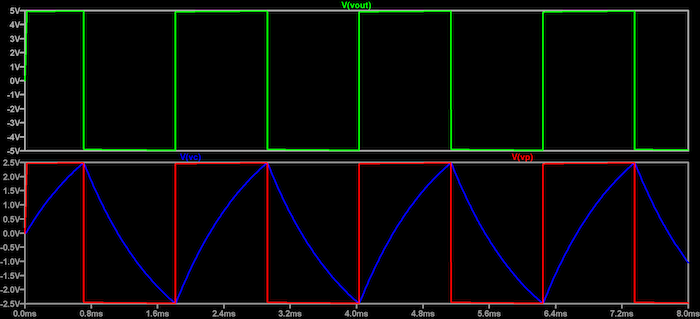
Figure 2. Op-amp astable multivibrator square wave oscillator simulation. Top: VOUT (green). Bottom: Vc (blue) and Vp (red)
As we can see, Vc charges and discharges to the trip points defined earlier by the resistor voltage divider between R1 and R2 and the supply voltages. The trip points, Vhigh and Vlow, are defined as:
$$ V_{high} = V_{p1}= 5(\frac{10 \text{ k}}{10 \text{ k} + 10 \text{ k}}) = 2.5 \text{ V}$$
$$ V_{low} = V_{p2}= -5(\frac{10 \text{ k}}{10 \text{ k} + 10 \text{ k}}) = -2.5 \text{ V}$$
The frequency of the waveform in Figure 2 is 451 Hz. It is defined by the RC time constant of R3 and C in Figure 1 required to charge and discharge the capacitor between Vhigh and Vlow.
To accurately calculate the frequency of the circuit in terms of the components, we must utilize the charging/discharging equation of an RC circuit. The general form of the charging equation is:
$$V(t)=V_{max}+(V_{initial} -V_{max})e^{\frac{-t}{\tau}}$$
Solving for t in this equation, we obtain:
$$t=-\tau \cdot ln(\frac{V_{max}-V(t)}{V_{max}-V_{initial}})$$
Now, if we assume the time to charge from Vlow to Vhigh, with Vmax = VDD, and we double the time to account for charge and discharge, we obtain the output period:
$$T = 2t = -2 \tau \cdot ln(\frac{V_{DD}-V_{up}}{V_{DD}-V_{low}}) = - 2RC \cdot ln(\frac{V_{DD}(1-\frac{R_1}{R_1 + R_2})}{V_{DD}-V_{SS} \frac{R_1}{R_1+R_2}})$$
This equation shows that the RC time constant dominates, while the values of R1 and R2 have a weak relationship to the period because they change the trip points to which the capacitor must charge and discharge.
If we plug in the values of R1, R2, R3, and C, we get a period of 455 Hz, which matches nearly our frequency of 451 Hz from the simulation.
This circuit is simple, effective, and supports both low and high frequencies, limited by the op-amp’s slew rate driving the output during the switching events. The downside is that the output swing cannot be made smaller, thereby setting a hard limit on the frequency as the output must swing from rail to rail.
To build this circuit with a single supply op-amp that swings from the ground (0 V) to VDD, the ground nodes connected to the capacitor and resistor R1 must be changed to a mid-range voltage—typically $$\frac{V_{DD}}{2}$$.
Transistor-based Square Wave Oscillator Using a BJT
An astable multivibrator can also be made with discrete transistors instead of the op-amp. An example using bipolar junction transistors (BJTs) is illustrated in Figure 3.
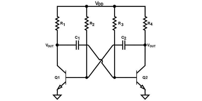
Figure 3. BJT-based astable multivibrator for square wave generation.
Upon startup of this circuit, one transistor, let’s assume Q2, will go into the “cut-off” region, where it conducts no current. This will cause the collector node (top of Q2) to charge up to VDD.
Meanwhile, Q1 will be saturated and thus conducting current. This will cause the node of C1 connected to the base of Q2 to charge up through R3 until Q2 is pushed into saturation. Upon being pushed to saturation, the sharp voltage drop on the right side of C2 causes a heavy negative response at the base of Q1, pushing it into cut-off.
This kind of push-pull behavior happens continuously, creating output voltage waveforms on both collectors of Q1 and Q2. The outputs are square waves of the same frequency but opposite phases. Since the bases of Q1 and Q2 charge/discharge via RC circuits of R3 with C1 and R2 with C2, respectively, we can define the output period of the generator as:
$$T=t_1+t_2$$
$$t_1=0.69R_3C_1$$
$$t_2=0.69R_2C_2$$
In the transient waveforms, t1 is the pulse width of the output at collector Q1, while t2 is the pulse width at collector Q2. As one can see in the equations, t1 need not be equal to t2, and thus we can create rectangular waveforms of variable duty cycle.
This behavior is demonstrated in the simulation results of Figure 4. For this simulation, we have designed the circuit to have a 50% duty cycle with t1 = t2.
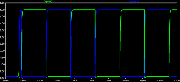
Figure 4. Bipolar transistor astable multivibrator output with symmetric outputs.
The components values for this simulation are:
- R1 = R4 = 1 kΩ
- R2 = R3 = 100 kΩ
- C1 = C2 = 10 nF
The BJTs are standard 2N2222 NPNs. Therefore our expected time constants from our basic equation are:
$$t_1 = t_2 = 0.69RC = 0.69(100 \text{ k}\Omega)(10 \text{ nF}) = 690 \text{ } \mu s $$
The measured result from our simulation is 681 μs which is close to our design value of 690 μs.
We can also change this design to have nonsymmetric performance. If we halve the resistance of R2 to 50 kΩ, we can change the period of t2 to 345 us. The simulation result for this circuit after the change is shown in Figure 5.
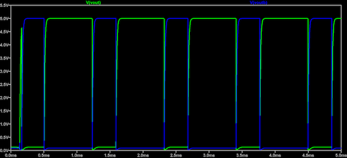
Figure 5. Bipolar transistor astable multivibrator output with nonsymmetric outputs.
From Figure 5, we see the ability to create nonsymmetric output rectangular waves with easily adjustable duty cycles. The simulation results are t1 = 681 μs and t2 = 335 μs which is again close to those predicted by our design equations.
Overall, the BJT-based astable multivibrator has much more flexibility when compared to the op-amp oscillator. While slightly more complex in structure, it does not require a negative power supply and produces both the output and its complement. It also gives the ability to form generic rectangular waves of variable frequency and duty cycle instead of pure square waves of variable frequency.
Review of Analog Square Wave Generator Circuits
Analog implementations of square wave oscillators rely on feedback mechanisms via RC charging/discharging that define the square wave frequency. While not limited to pure square waves, as seen in the BJT version of the astable multivibrator, both of these circuits allow for highly configurable square waveforms to be generated via a simple circuit with no reference signal required.
Related Content


My favorite implementation of the “op-amp” generator is with a CMOS 555. The Trigger and Threshold pins tied together become the input of a Schmidt trigger that switches at 2/3 and 1/3 of Vcc. Cap to ground and a feedback resistor. Plenty of output drive, even more available at the Discharge pin.
my favorite