Facebook
 Google
 GitHub
 Linkedin
Understanding Dynamic Range and Spurious-Free Dynamic Range in RF Systems
Learn to calculate the upper and lower limits of a circuit’s dynamic range and spurious-free dynamic range (SFDR).
At very low input powers, the output of a circuit isn’t deterministic—it’s produced by the circuit’s noise, not as an intended response to the input signal. As the input signal level increases, however, the circuit becomes more and more nonlinear. Eventually, the output may no longer be a faithful reproduction of the input.
Dynamic range and spurious-free dynamic range (SFDR) both characterize the range of power levels that a circuit can process with acceptable quality, meaning that the output is both deterministic and an acceptably linear replica of the input. In this article, we’ll examine these two performance parameters in the context of RF systems. More specifically, we’ll explore how the upper and lower bounds of the input signal amplitude are determined for both specifications.
Dynamic Range
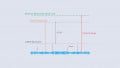
For the dynamic range metric, the minimum permissible signal is defined as the output noise floor and the maximum permissible signal is defined as the circuit’s 1 dB compressed output power. This specification, which is sometimes called linear dynamic range, is illustrated in Figure 1.

Figure 1. Visual representation of the dynamic range specification. Image used courtesy of Steve Arar
The 1 dB compression point is typically provided by the datasheet. However, the noise floor must be calculated. To do so, we can use the following equation for the noise factor (F):
$$F~=~\frac{N_o}{GN_i}$$
Equation 1.
where:
Ni is the noise at the circuit’s input
No is the total noise at the output
G is the power gain of the stage.
No includes both the effect of the internal noise sources within the circuit and the noise from the source impedance. More specifically, Ni is the available thermal noise power of the source resistor at a temperature of T0. It’s given by:
$$N_i ~=~ kT_0B$$
Equation 2.
where:
k is Boltzmann’s constant (1.38 × 10⁻²³ joules/K)
T0 = 290 K
B is the bandwidth in hertz.
Substituting Equation 2 into Equation 1 and solving for No, the output noise is:
$$N_o ~=~ G ~\times~ kT_0 B ~\times~ F$$
Equation 3.
Expressing the quantities in decibels, we obtain:
$$N_o \Big |_{\text{dBm}} ~=~ G \Big |_{\text{dB}} ~-~ 174 \ \text{dBm/Hz} ~+~ 10 \log(B)~+~NF \Big |_{\text{dB}}$$
Equation 4.
where:
–174 dBm/Hz is the approximate value of 10log(kT0)
NF is the noise figure.
Having determined the output noise floor, the linear dynamic range is calculated as:
$$DR ~=~ P_{out,1 \text{dB}}~-~N_o$$
Equation 5.
Example 1: Determining the Dynamic Range
To cement the above concepts, let’s consider an amplifier with the following characteristics:
- A gain of G = 30 dB.
- A noise figure of NF = 2.5 dB.
- A 1 dB compression point of Pout,1dB = 20 dBm.
If the noise bandwidth is 1 GHz, what is the amplifier’s dynamic range?
First, we use Equation 4 to calculate the noise floor:
$$\begin{eqnarray}N_o \Big |_{\text{dBm}} &~=~& G \Big |_{\text{dB}} ~-~ 174 \ \text{dBm/Hz} ~+~ 10 \log(B)~+~NF \Big |_{\text{dB}} \\&~=~& 30~-~174~+~10\log(10^9)~+~2.5~=~-51.5 \ \text{dBm}\end{eqnarray}$$
Equation 6.
Then, we calculate the dynamic range:
$$DR~=~ P_{out,1\text{dB}}~-~N_o~=~20~-~(-51.5)~=~71.5 \ \text{dB}$$
Equation 7.
As we see above, the dynamic range works out to 71.5 dB.
Applications and Limitations of the Dynamic Range Specification
The dynamic range specification uses the 1 dB compression point—a linearity metric that uses a single-tone input—to assess whether or not the circuit is acceptably linear. Since most practical RF systems process input signals consisting of many frequencies, this limits the dynamic range specification’s usefulness.
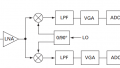
Despite its limitations, the dynamic range plays an important role when measuring the frequency response of RF components. Measurements of this kind are conducted using a vector network analyzer (VNA) like the one in Figure 2.

Figure 2. Basic VNA block diagram. Image used courtesy of David M. Pozar
Figure 3 shows how the measured frequency response of a highly selective filter can be influenced by the VNA’s dynamic range.

Figure 3. Frequency response of a bandpass filter measured using a VNA with poor dynamic range (left) and good dynamic range (right). Image used courtesy of Agilent Technologies
In the above example, the filter has a stopband rejection of 90 dB. The left-hand measurement is conducted using a VNA with a sensitivity of about –60 dB. The poor dynamic range results in VNA mostly measuring its own noise floor rather than the filter’s stop-band behavior.
In the right half of the figure, the same filter is measured using a VNA with a sensitivity of –100 dBm. The increased dynamic range allows us to more accurately measure the filter’s stopband response.
It should be noted that while basic S-parameter measurements use a single-tone test signal, more advanced measurements may need multi-tone inputs or modulated signals to characterize the device under test more completely. In these cases, the dynamic range specification may not fully reflect the VNA’s linearity performance.
An Alternative Definition of Minimum Permissible Signal
Previously, we defined the minimum permissible signal as being equal to the noise floor. Sometimes, however, we may instead define it as being a few decibels above the noise floor. For example, the book “Fundamentals of RF and Microwave Transistor Amplifiers” by Inder Bahl assumes that the minimum detectable signal at the amplifier’s output is typically 3 dB higher than the output noise floor.
Let’s see how Bahl’s definition changes the results of Example 1. Since the output noise floor was –51.5 dBm (Equation 6), we would now consider the minimum detectable signal at the output to be –48.5 dBm. The dynamic range is therefore reduced by 3 dB, from 71.5 dB to 68.5 dB:
$$DR= P_{out,1\text{dB}}~-~N_o~=~20~-~(-48.5)~=~68.5 \ \text{dB}$$
Equation 8.
This alternative definition is primarily beneficial when assessing the performance of receiver systems rather than individual components. A receiver’s minimum detectable signal depends on several system-level parameters, including:
- Modulation scheme.
- Bit rate.
- Energy per bit.
- Filter bandwidth.
It’s therefore useful to consider a margin between the minimum detectable signal and the noise floor.
Before we move on, note that we can refer both the minimum and maximum power levels to the input and compute the dynamic range. Since both the minimum and maximum power levels are changed by the same gain factor when referenced to the input, the result is the same.
Spurious-Free Dynamic Range
Let’s turn our attention to a different performance metric, the spurious-free dynamic range (SFDR). For this specification, the minimum permissible signal is simply the noise floor. The definition of the maximum permissible signal is a bit more complicated. To understand it, consider Figure 4.

Figure 4. A visual representation of the SFDR specification. Image used courtesy of Steve Arar
Figure 4 shows the power of the fundamental output component and the third-order intermodulation (IM3) component vs. the input power. It also shows the output noise floor. As we can see, the fundamental component exhibits a slope of 1:1. The IM3 product, on the other hand, rises 3 dB for every 1 dB increase in the input power.
As the input power increases, the IM3 product becomes larger and larger. Eventually, it reaches a point (PIM3) where its power is equal to that of the noise floor. The input power associated with this point is denoted by P1.
When the input power exceeds P1, the SFDR specification considers operation to be excessively nonlinear. The maximum permissible signal is therefore PF, the output power associated with P1. Recalling that PIM3 is equal to the noise floor, the SFDR can be defined in mathematical terms as:
$$SFDR~=~P_F~-~P_{IM3}$$
Equation 9.
By taking the slopes of the fundamental and IM3 components into account, we can express the above equation in terms of the third-order intercept point (IP3).
First, let's define ΔP as the difference between the input IP3 point (IIP3) and P1. This is shown along the bottom of Figure 4. Since the IM3 power rises with a slope of 3:1, the difference between the output IP3 point (OIP3) and PIM3 is 3ΔP. We can therefore represent Equation 9 as:
$$SFDR ~=~ P_F ~-~ P_{IM3} ~=~ 2 \Delta P ~=~ 2 ~\times~ (IIP3 ~-~ P_1)$$
Equation 10.
Also, since the slope of the linear output is unity, the difference between OIP3 and PF is ΔP. Like the difference between OIP3 and PIM3, this can be seen along the right edge of Figure 4. The SFDR, being the difference between PF and PIM3, is therefore equal to 2ΔP:
$$SFDR ~=~ P_F ~-~ P_{IM3} ~=~ 2 \Delta P$$
Equation 11.
Combining Equations 10 and 11, we have:
$$SFDR ~=~ \frac{2}{3} (OIP3~-~N_o)$$
Equation 12.
The SFDR is the most commonly utilized and beneficial specification for characterizing the dynamic range of RF circuits. This is because the third-order nonlinearity is usually the primary distortion mechanism affecting the circuit. Consequently, enhancing the system’s SFDR should be a principal design objective.
Example 2: Determining the SFDR
Consider an amplifier with the following characteristics:
- Available power gain of G = 30 dB.
- Noise figure of NF = 5 dB.
- Output third-order intercept point of OIP3 = 30 dBm.
If the noise bandwidth is 500 MHz, what is the SFDR of the amplifier?
From Equation 4, the output noise floor is:
$$\begin{eqnarray}N_o \Big |_{\text{dBm}} &~=~& G \Big |_{\text{dB}} ~-~ 174 \ \text{dBm/Hz}~ +~ 10 \log(B)~+~NF \Big |_{\text{dB}} \\&~=~& 30~-~174~+~10\log(500 ~\times~ 10^6)~+~5 \\&~=~& -52 \ \text{dBm}\end{eqnarray}$$
Equation 13.
We can now calculate the SFDR:
$$SFDR ~=~ \frac{2}{3} (OIP3~-~N_o)~=~\frac{2}{3} (30~-~(-52))~=~54.67 \ \text{dB}$$
Equation 14.
The SFDR of this amplifier is 54.67 dB.
Wrapping Up
The dynamic range is a crucial specification for system designers. Similar to how a circuit’s bandwidth must be sufficiently broad to accommodate the input frequencies, its dynamic range must be high enough to ensure it can accurately process the varying power levels it receives. In this article, we discussed two different ways of characterizing the dynamic range to suit the needs of different applications.
This article is Part 8 in a series on linearization techniques and nonlinearity in RF systems. Below is a complete list of articles in this series:
- Introduction to the Feed-Forward Linearization of RF Power Amplifiers
- Using Analog Predistortion for RF Power Amplifier Linearization
- Improving RF Power Amplifier Linearity With Digital Predistortion
- Introduction to the Memory Effect in RF Power Amplifiers
- Using the 1 dB Compression Point to Characterize RF System Nonlinearity
- Understanding Intermodulation Distortion and the Third-Order Intercept Point in RF Systems
- A Guide to Calculating IM3 and IP3 for Nonlinear RF Circuits
- Understanding Dynamic Range and Spurious-Free Dynamic Range in RF Systems
- Understanding the Third-Order Intercept Point of a Cascaded System
- Dynamic Nonlinearity in RF Power Amplifiers: Insights From Two-Tone Testing