Facebook
 Google
 GitHub
 Linkedin
Discrete Semiconductor Devices and Circuits
Class A BJT Amplifiers
62 questions By Tony R. Kuphaldt
-
Question 52 of 62
In a common-collector transistor amplifier circuit with voltage divider biasing, the input impedance (Zin) is a function of load impedance, emitter resistance (RE), and the two biasing resistances (R1 and R2). Often, the biasing resistances are of sufficiently low value to swamp the input impedance of the transistor, so that R1 and R2 constitute the heaviest load for any input signals driving the amplifier.

$$Z_{in} \approx R_1 || R_2 || (\beta +1)[r’_e+(R_E||R_{load})]$$
This is a shame, because the only practical purpose served by R1 and R2 is to provide a stable bias voltage so the transistor always functions in class A mode. In order to provide a stable bias, these resistors have to be relatively low in value compared to the impedance seen at the base of the transistor (resulting from the load). Otherwise, changes in dynamic emitter resistance (r′e) could result in significant bias shifts. So, the naturally high input impedance of the common-collector transistor configuration is spoiled by the necessary presence of R1 and R2.
A clever way to recover some of that naturally large input impedance is to add a bit of regenerative (positive) feedback to the circuit in the form of a capacitor and another resistor. This technique is given an equally clever name: bootstrapping.
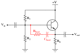
Explain how bootstrapping works, and why that particular name is given to the technique.
Reveal answerBy feeding some of the emitter signal to the base of the transistor, the transistor helps drive itself, reducing the load on the signal source (connected at Vin). This is analogous to the fanciful scenario of someone making themselves lighter by pulling up on their own bootstraps.
Notes:Bootstrapping is an oft-used technique to boost amplifier input impedance, and it hints at the amazing potential of signal feedback in amplifier circuits. You might want to mention that bootstrapping is practical only if the feedback gain is slightly less than 1. If there is too much positive feedback, the amplifier will turn into an oscillator!
-
Question 53 of 62
A common set of equations for calculating input and output impedances of common-collector amplifier circuits is as follows:
$$Z_{in} \approx R_1 || R_2 || (\beta +1)[r’_e+(R_E||R_{load})]$$
$$Z_{out} \approx R_E || (r’_e+\frac{R_1||R_2||R_{source}}{\beta +1})$$
If precision is not required, we may greatly simplify these equations by assuming the transistor to be ideal; i.e. having an infinite current gain (β = ∞). Re-write these equations accordingly, and explain how you simplified each one.
Reveal answer$$Z_{in} \approx R_1 || R_2$$
$$Z_{out} \approx R_E || r’_e$$
Much simpler, don’t you think?
Notes:The purpose of this question is for students to see how (more) approximate predictions for circuits may be obtained through simplification. A good exercise is to calculate impedances for a given amplifier circuit using both the original and the simplified equations, to see just how “approximate” the simplified answers are. Knowing how to eliminate complicated terms in equations (and what terms may be safely eliminated!) is key to estimating in the absence of a calculator.
-
Question 54 of 62
Approximate the following values for this common-collector amplifier circuit, assuming the use of a silicon transistor:

- AV (as a ratio) ≈
- AV (in decibels) ≈
- Zin ≈
- Zout ≈
Reveal answer- AV (as a ratio) ≈ 1
- AV (in decibels) ≈ 0 dB
- Zin ≈ 5.962 kΩ
- Zout ≈ 39.6 Ω
Follow-up question: how would these figures change, if at all, supposing the transistor had an infinite current gain \((\beta=∞)\)?
Notes:Nothing much to comment on here - just some practice on common-collector amplifier calculations. In calculating the dynamic emitter resistance, the following assumptions were taken:
- r′e = 25 mV / IE
- 0.7 volts drop (exactly) across base-emitter junction.
- Negligible loading of bias voltage divider by the emitter resistance.
After calculating r′e, the following equations were used to approximate the impedances:
$$Z_{in} \approx R_1 || R_2||(\beta+1)[r’_e+(R_E||R_{load})]$$
$$Z_{out} \approx R_E || (r’_e+\frac{R_1||R_2||R_{source}}{\beta +1})$$
This question lends itself well to group discussions on component failure scenarios. After discussing how to calculate the requested values, you might want to ask students to consider how these values would change given some specific component failures (open resistors, primarily, since this is perhaps the most common way that a resistor could fail).