Facebook
 Google
 GitHub
 Linkedin
Discrete Semiconductor Devices and Circuits
Class A BJT Amplifiers
62 questions By Tony R. Kuphaldt
-
Question 58 of 62
Approximate the following values for this common-emitter amplifier circuit, assuming the use of a silicon transistor:
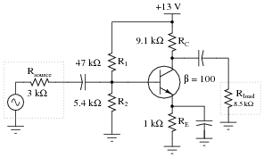
- AV (as a ratio) ≈
- AV (in decibels) ≈
- Zin ≈
- Zout ≈
Reveal answer- AV (as a ratio) ≈ 112.5
- AV (in decibels) ≈ 41.02 dB
- Zin ≈ 2.175 kΩ
- Zout ≈ 9.1 kΩ
Follow-up question: how would these figures change, if at all, supposing the transistor had an infinite current gain \((\beta=∞)\)?
Notes:Nothing much to comment on here - just some practice on common-emitter amplifier calculations. In calculating the dynamic emitter resistance, the following assumptions were taken:
- r′e = 25 mV / IE
- 0.7 volts drop (exactly) across base-emitter junction.
- Negligible loading of bias voltage divider by the emitter resistance.
After calculating r′e, the following equations were used to approximate the impedances:
$$Z_{in} \approx R_1||R_2||(\beta+1)r’_e$$
$$Z_{out} \approx R_C$$
Voltage gain was approximated through the use of this equation:
$$A_V \approx \frac{R_C||R_{load}}{r'_e}$$
This question lends itself well to group discussions on component failure scenarios. After discussing how to calculate the requested values, you might want to ask students to consider how these values would change given some specific component failures (open resistors, primarily, since this is perhaps the most common way that a resistor could fail).
-
Question 59 of 62
A parasitic property of semiconductor PN junctions is capacitance across the depletion regions. This is often referred to as the Miller Effect. In transistor circuits, the Miller effect contributes to a decrease in voltage gain as signal frequency increases.
Explain why junction capacitances make the voltage gain of an amplifier decrease with increasing frequency.
Reveal answerThe Miller capacitance between collector and base in a transistor forms a negative feedback loop for AC signals.
Challenge question: is there any way you can think of to cancel out this negative feedback in an amplifier circuit?
Notes:Ask your students to explain what a “negative feedback loop” is, and how exactly the base-collector junction capacitance forms one in a transistor circuit. Also, review the formula for capacitive reactance (XC), and ask your students to relate this frequency dependence to the degree of negative feedback established in an amplifier circuit.
The challenge question may be answered with a little research into the Miller-effect. There is a method for cancellation of this unwanted negative feedback loop, but it may not be possible to implement in all amplifier circuit topologies.
-
Question 60 of 62
The BJT amplifier configuration most affected by the Miller effect at high frequencies is the common-emitter. Common-collector and common-base amplifier configurations do not suffer the same great losses of voltage gain at high frequency as the common-emitter circuit does. After examining the following amplifier circuits (with the Miller effect capacitance shown external to the transistors), explain why:
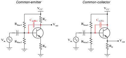
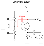
Reveal answerIn the common-emitter circuit, the Miller capacitance provides a path for the (inverted) output signal at the collector terminal to degeneratively feed back to the input at the base terminal, decreasing voltage gain. In the common-collector circuit, there is no signal inversion at all, and so no degenerative feedback can happen at all.
The common-base circuit is interesting: it would seem there is a possibility for negative feedback through the Miller capacitance here, from the collector to the base. However, since the base terminal is effectively grounded (as far as AC signals are concerned) by the bypass capacitor, any feedback through the Miller capacitance becomes shunted straight to ground where is has no effect on the amplifier’s operation.
Notes:Here I give more explanation than is usual for me, because the concept is not easy to understand, and is often presented in a muddled fashion by textbooks.