Facebook
 Google
 GitHub
 Linkedin
Unraveling the Design Equations of the Class E Power Amplifier
In this article, we analyze the operation of the Class E amplifier and examine the underlying assumptions of its design equations.
The Class E mode of operation allows us to build high-efficiency power amplifiers with output power levels that range from several kilowatts (at low RF frequencies) up to about one watt (at microwave frequencies). Simplicity of design is one of the Class E amplifier’s main advantages—unlike other amplifier classes, it demands minimal adjustments after the initial design phase to achieve satisfactory performance.
A comprehensive analysis of Class E operation would require some rather lengthy and tedious mathematics. Instead, this article will use simplifying assumptions to create a streamlined version of the analysis and derive the Class E power amplifier’s basic design equations. Though we presented most of these equations in the previous article, the distilled analysis included here should help you confidently apply them to your application.
After we complete the circuit analysis, we’ll examine how our starting assumptions affect the results. This section will also provide a list of references and reading recommendations for those who want a more in-depth treatment.
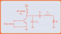
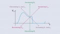
Figure 1 shows the basic Class E stage we’ll be examining. Its typical switch waveforms are shown in Figure 2.

Figure 1. Schematic of a basic Class E amplifier.
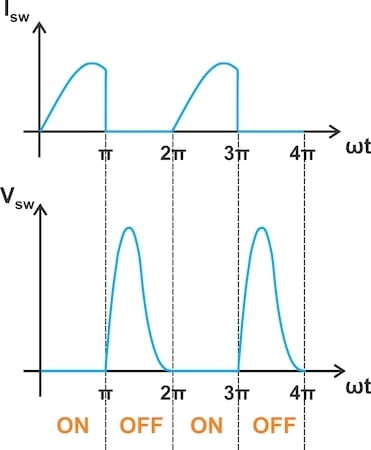
Figure 2. Typical switch current (top) and switch voltage (bottom) waveforms in a Class E amplifier.
These figures may already be familiar to you from earlier articles in this series. They are reproduced here for convenience, as we’ll refer back to them throughout our discussion.
With that, let’s begin our analysis.
Finding the Voltage Across the Shunt Capacitor
Assuming that the load network’s Q-factor is high enough, the Class E amplifier’s output current is sinusoidal at the switching frequency. The load current is given by:
$$i_{R} ~=~ I_{R} \sin(\omega t ~+~ \phi)$$
Equation 1.
where IR is the peak value of the current and ϕ is its initial phase.
The RF choke provides a DC path to the supply and approximates an open circuit at RF. In Figure 3, the DC current through the RF choke is denoted by I0.
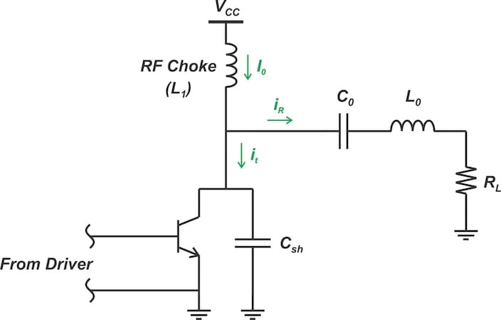
Figure 3. The RF choke supplies a DC current of I0 and the sinusoidal current iR flows through the load.
In the above figure, the total current flowing through the switch and shunt capacitor is:
$$i_{t} ~=~ I_0 ~-~ I_{R} \sin(\omega t ~+~ \phi)$$
Equation 2.
The current flowing through the switch and capacitor is therefore an offset sine wave.
Suppose that for the time interval 0 < ⍵t < π, the switch is ON. During this interval, it passes entirely through the switch. Assuming that the saturation voltage of the switch is negligible, the collector voltage is at ground potential.
In the next half-cycle (π < ⍵t < 2π), the switch is open and it flows entirely through the capacitor. The voltage across the shunt capacitor (vc) when the switch is OFF can be found by integrating it over the relevant time interval:
$$v_c ~=~ \frac{1}{C_{sh} \omega} \int_{\pi}^{\omega t} I_0 ~-~ I_{R} \sin(\omega t ~+~ \phi) \ d(\omega t)$$
Equation 3.
which leads to:
$$v_c ~=~ \frac{1}{C_{sh} \omega} \bigg ( I_0 (\omega t ~-~ \pi) ~+~ I_{R} \big ( \cos(\omega t ~+~ \phi) ~+~ \cos(\phi) \big ) \bigg ) ~+~ A$$
Equation 4.
where A is a constant of integration.
Before we proceed, note that the switch current is diverted to the shunt capacitor at the instant the switch opens. This is a definitive aspect of ideal Class E operation.
Applying Zero Value and Zero Derivative Conditions
During the time interval 0 <⍵t < π, the switch is ON, and the collector voltage is at ground potential. Just after ⍵t = π, the voltage across the shunt capacitor is zero. Applying this condition to Equation 4 leads to A = 0.
In a Class E stage, the voltage across the switch/capacitor is also zero when the switch turns ON. Therefore, vc must be zero at ⍵t = 2π (see Figure 2). From Equation 4, we obtain:
$$\cos(\phi) ~=~ -\frac{\pi I_0}{2 I_R}$$
Equation 5.
Furthermore, in an ideal Class E stage, the slope of the switch/capacitor voltage is zero at the instant the switch turns ON. Taking the derivative of Equation 4 with respect to ⍵t and equating it with zero at ⍵t = 2π, we have:
$$\frac{d v_c}{d (\omega t)} ~=~ 0 ~\rightarrow~ I_0 ~-~ I_R \sin(\omega t ~+~ \phi)~=~0$$
Equation 6.
This produces another useful relationship between the circuit parameters:
$$\sin(\phi)~=~\frac{I_0}{I_R}$$
Equation 7.
Finally, we combine Equations 5 and 7 and use the tangent equation to determine the current’s initial phase:
$$\tan(\phi)~=~ \frac{\sin{(\phi)}}{\cos{(\phi)}} ~=~-\frac{2}{\pi} ~\rightarrow ~\phi ~=~ 147.52 ~\text{degrees}$$
Equation 8.
Accounting for 100% Efficiency
With ideal components, the Class E amplifier has an efficiency of 100%. This is because the switch voltage and current waveforms don’t overlap, reducing the switch power loss to zero. This means that all of the DC power provided by the supply is delivered to the load:
$$V_{cc} I_0 ~=~ \frac{1}{2} R_L I_R^2$$
Equation 9.
Combining this equation with Equation 7, we find the load current:
$$I_R ~=~ 2 \sin(\phi) \frac{V_{cc}}{R_L}~=~ 1.074 ~\times~ \frac{V_{cc}}{R_L}$$
Equation 10.
and the DC current flowing through the RF choke:
$$I_0 ~=~ 2 \sin^2(\phi) \frac{V_{cc}}{R_L}~=~ 0.577 ~\times~ \frac{V_{cc}}{R_L}$$
Equation 11.
Finding the Shunt Capacitance and the Load Network Inductance
So far, we’ve calculated the initial phase of the load current (ϕ = 147.52 degrees) and found expressions that relate I0 and IR to the supply voltage and load resistance. Next, let’s find the required shunt capacitance (Csh).
There are a few different ways we could go about this. In one method, we start by noting that the DC component of the voltage across the ideal RF choke is zero. The DC value of the voltage across the switch and shunt capacitor must therefore be equal to the supply voltage:
$$V_{cc} ~=~ \frac{1}{2 \pi} \int_{\pi}^{2 \pi} v_c d(\omega t)$$
Equation 12.
Substituting vc from Equation 4 and using some algebra produces:
$$C_{sh} ~=~ \frac{0.1836}{\omega R_L}$$
Equation 13.
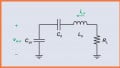
An alternative method involves identifying the fundamental component of the switch/capacitor voltage. I find this method more appealing, as it allows us to determine not only Csh but also other components—namely, L0 and C0—of the circuit in Figure 1. To understand this method, we need to examine the load network at the fundamental frequency (Figure 4).

Figure 4. A model of the Class E amplifier's load network at the fundamental frequency.
In the above diagram, L is the effective inductance that the series resonant circuit presents at the fundamental frequency. L is not to be confused with L0—it includes the effect of both L0 and C0. As we discussed in the previous article, the Class E amplifier’s load reactance at the operating frequency is non-zero and comparable in value to the load resistance (RL). The other RF amplifier classes we’ve examined commonly use a resonant circuit tuned to the frequency of operation, leaving them with zero load reactance at the fundamental frequency.
Let’s get back to analyzing the network in Figure 4. Our present goal is to determine the value of Csh and L in terms of RL. We know that the current flowing through the network is a sinusoid with amplitude IR and initial phase ϕ, and that the voltage across the shunt capacitor is given by Equation 4.
We can use either the frequency domain or the time domain approach to solve this problem. I’ll use the time domain method, as I find it more intuitive. Figuring out the voltage across RL is a breeze:
$$v_{R} ~=~ R_L ~\times~ i_R~=~ R_L I_R \sin(\omega t ~+~ \phi)$$
Equation 14.
The voltage across an ideal inductor leads its current by exactly 90 degrees. Since the current is expressed as a sine function, the voltage across the inductor is a cosine function of time:
$$v_{L} ~=~ L \omega ~\times~ I_R \cos(\omega t ~+~ \phi)$$
Equation 15.
Therefore, the voltage across the shunt capacitor at the fundamental frequency is:
$$v_c ~=~ v_R ~+~ v_{L} ~=~ R_L I_R \sin(\omega t ~+~ \phi) ~+~ L \omega I_R \cos(\omega t ~+~ \phi)$$
Equation 16.
This means that the voltage across the shunt capacitor consists of two components:
- A component that’s in phase with the output current.
- A component that’s a cosine function of time (the quadrature component).
We can find both of these components by applying a Fourier analysis. The in-phase component (vci) is calculated as follows:
$$v_{ci} ~=~ \frac{1}{\pi}\int_{\pi}^{2 \pi} v_c \sin(\omega t ~+~ \phi) \ d(\omega t)$$
Equation 17.
Similarly, the quadrature component (vcq) is given by:
$$v_{cq} ~=~ \frac{1}{\pi}\int_{\pi}^{2 \pi} v_c \cos(\omega t ~+~ \phi) \ d(\omega t)$$
Equation 18.
By performing some basic—if somewhat lengthy—calculations, we can simplify Equations 17 and 18 to produce the following:
$$v_{ci} ~=~ -\frac{I_R}{\pi C_{sh} \omega} \bigg (\frac{\pi}{2} \sin(2 \phi) ~+~ 2 \cos(2 \phi) \bigg )$$
Equation 19.
and:
$$v_{cq} ~=~ \frac{I_R}{\pi C_{sh} \omega} \bigg (\pi \sin^2(\phi) ~+~ 2 \sin(2 \phi) ~+~ \frac{\pi}{2} \bigg )$$
Equation 20.
From Equation 16, the peak values of the in-phase and quadrature components are, respectively, RLIR and L⍵IR. Setting vci equal to RLIR and using ϕ = 147.52 degrees leads to:
$$C_{sh} ~=~ \frac{0.1836}{\omega R_L}$$
Equation 21.
which is identical to Equation 13.
Finally, equating vcq with L⍵IR and using ϕ = 147.52 degrees gives us:
$$LC_{sh} \omega^2 ~=~ 0.2116$$
Equation 22.
Finding L0 and C0
Now we’re in a position to find L0 and C0, the components of the series resonant circuit. With a given Q-factor for the load network, we can use the following equation to determine the value of L0:
$$L_{0} ~=~ \frac{Q R_L}{\omega}$$
Equation 23.
The effective inductive reactance at the fundamental frequency is:
$$L \omega ~=~ L_0 \omega ~-~ \frac{1}{C_0 \omega}$$
Equation 24.
where L and L0 are given by Equations 22 and 23, respectively. Equation 24 is sometimes also written as:
$$\frac{1}{C_0 \omega} ~=~ L_0 \omega ~-~ \frac{0.2116}{C_{sh} \omega}$$
Equation 25.
Examining Our Assumptions
Now that we’ve derived the design equations, it’s time to consider the assumptions we made in the above analysis:
- A Q-factor high enough to produce a sinusoidal output current.
- A 50% duty cycle.
- A switch with zero ON-resistance, infinite OFF-resistance, and instantaneous switching time.
- Lossless passive components, including an ideal RF choke.
Let’s examine each of these more closely.
A High Q-Factor and a Sinusoidal Output Current
Throughout the analysis, we assumed that the output current is sinusoidal at the switching frequency. Technically, this would require the quality factor (Q) of the load network to be infinitely high. Practical values of Q range from 3 to 10, allowing some harmonic current to flow into the load network. The lower Q is, the less accurate our assumption regarding the output current becomes.
If we use the derived equations in a design with an insufficiently high Q, we may not be able to achieve the zero voltage and derivative switching conditions we need for optimum operation. For a comprehensive analysis that doesn’t assume a high Q, please refer to “Exact analysis of class E tuned power amplifier at any Q and switch duty cycle” by M. Kazimierczuk.
A 50% Duty Cycle
Though we assumed a duty cycle of 50%, this isn’t a fundamental requirement of Class E operation. However, it’s more complicated to analyze the circuit for arbitrary duty cycle values.
For those who are interested, an analysis for any duty cycle value can be found in F. Raab’s classic paper “Idealized operation of the class E tuned power amplifier.” The book “RF Power Amplifiers for Wireless Communications” by Dr. Steve Cripps, which may be more approachable for beginners, also analyzes the Class E amplifier for an arbitrary duty cycle.
Ideal Circuit Components
We assumed that our components—the switch, the RF choke, the series inductor, and the capacitors—were ideal. However, a real-life switch won’t have zero ON-resistance, infinite OFF-resistance, or an instantaneous switching time. We’ll also see some power loss due to the equivalent series resistance of the inductors and capacitors. Because of these non-idealities we need to account for turn-OFF switching loss in our design even when the zero-voltage switching condition is satisfied and the turn-ON switching loss is zero.
Finally, we assumed that only DC current flowed through the RF choke. This would require a choke with infinite reactance, which isn’t practically feasible.
Wrapping Up
In this article, we walked through a simplified analysis of the Class E amplifier. If you’re interested in delving more deeply into this topic, I have included a list of references below:
- “RF Power Amplifiers” by M. K. Kazimierczuk.
- “Switchmode RF and Microwave Power Amplifiers” by A. Grebennikov, N. O. Sokal, and M. J. Franco.
- “Radio-Frequency Electronics Circuits and Applications” by J. B. Hagen.
In the next article, we’ll explore how a practical Q-factor—typically between 3 and 10—results in the flow of harmonic currents into the load. We’ll then discuss how this issue can be addressed.
This article is Part 16 of a series on power amplifier classes. A complete list of articles in this series is provided below.
Classes A through C:
Class D:
Class E:
Class F and Inverse Class F:
Featured image used courtesy of Adobe Stock; all other images used courtesy of Steve Arar