Facebook
 Google
 GitHub
 Linkedin
Digital Circuits
Latch Circuits
26 questions By Tony R. Kuphaldt
-
Question 7 of 26
The following relay logic circuit is for starting and stopping an electric motor:

Draw the CMOS logic gate equivalent of this motor start-stop circuit, using these two pushbutton switches as inputs:

Make sure that your schematic is complete, showing how the logic gate will drive the electric motor (through the power transistor shown).
Reveal answer
Follow-up question: why is the “Stop” switch always normally-closed in motor control circuits, whether it be relay logic or semiconductor logic? It is easy enough to invert a signal if we wish to, either by using a relay or by using a NOT gate, so shouldn’t the choice of switch “normal” status be arbitrary?
Challenge question: why not operate the electric motor off the same VDD power source that the gates are powered by? If we had to do such a thing, what circuit additions would you propose to minimize any potential trouble?
Notes:Discuss the follow-up question with your students. Why is the “Stop” switch always normally-closed, if we have the freedom to choose normally-open contacts? Why not standardize the pushbutton switches, making them both the same type? The answer has to do with circuit faults, and what is considered the safest mode of failure.
I suspect many students will neglect to include the base resistor in their designs. This resistor is important, though, for the sake of the driving gate. You might even want to spend some class time with your students calculating an appropriate value of resistance, given such parameters as:
- Motor “run” current = 300 mA
- Transistor β = 50
- VDD = 6 volts DC
The challenge question may be too advanced for students who have not yet experienced the pains of trying to operate power devices and logic devices off the same DC bus. Suffice it to say, it is a good design rule to keep separate DC power supplies for logic and load circuitry, even if they are the exact same voltage!
-
Question 8 of 26
One practical application of S-R latch circuits is switch debouncing. Explain what “bounce” refers to in mechanical switches, and also explain how this circuit eliminates it:

Also, show where an oscilloscope could be connected to display any switch “bounce,” and explain how the oscilloscope would have to be configured to capture this transient event.
Reveal answerThe “latching” ability of the S-R latch circuit holds the output state steady during the mechanical switch’s bouncing action, allowing a “clean” output transition to take place.
Connecting the input probe of an oscilloscope to either the S or R input of the latch will show bounce, if it occurs. To capture this event, the ‘scope would have to be configured for single-sweep mode, and have the triggering controls properly set. A digital storage oscilloscope is essential for this type of work!
Follow-up question: how do you suggest choosing appropriate pull-down resistor sizes for this circuit, or any CMOS circuit for that matter?
Notes:Many textbooks use switch debouncing as a practical example of S-R latch function, so I won’t bother giving hints as to how this circuit works. Let the students do their own research, and let them explain it to you during discussion.
If students need practical examples of how switch “bouncing” can be bad, suggest digital counter circuits, where a mechanical switch causes a counter to increment (or decrement) once per actuation. If the switch bounces, the counter will increment (or decrement) more than once per switch actuation, which is undesirable.
Oscilloscope triggering is one of those features that separates novice ‘scope users from competent ‘scope users. Anyone can learn to display a repetitive waveform on an oscilloscope with a minimum of adjustment. Many modern digital oscilloscopes even have “auto-configure” features to lock in such waveforms for display. However, to set up triggering on one-time events requires that the user understand not only the oscilloscope’s functions, but also the nature of the event to be captured.
Note to your students how the [Q] output of the latch doesn’t go anywhere. Often, we have applications where the second output of a latch is unused. Ask your students whether or not this constitutes a problem. (If you get blank stares from asking this question, remind students that unused CMOS inputs have to be grounded or tied to VDD, or else damage may occur. Ask them whether or not the same rule applies to gate outputs.) This will be a good review of internal gate circuit construction.
-
Question 9 of 26
Complete the timing diagram, showing the state of the Q output over time as the Set and Reset switches are actuated. Assume that Q begins in the low state on power-up:
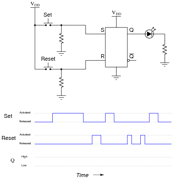
Reveal answer
Follow-up question: complete a schematic diagram showing how the [Q] output of the latch could turn on an electric motor through a bipolar junction transistor. Also, determine whether the latch circuit would be sourcing or sinking current to the transistor when the motor is running:

Notes:Nothing special here in this question. Perhaps the main point is to familiarize students with the concept of a timing diagram, and how to transfer the truth table function of a specific logic circuit to a time-domain plot.