Facebook
 Google
 GitHub
 Linkedin
Digital Circuits
Latch Circuits
26 questions By Tony R. Kuphaldt
-
Question 16 of 26
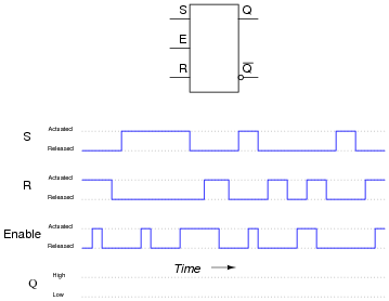
Complete the timing diagram, showing the state of the Q output over time as the input switches are actuated. Assume that Q begins in the low state on power-up:
Reveal answer
Notes:Have your students explain exactly how they arrived at the solution they did for the output waveform. Are they making use of a truth table for the S-R latch to figure out what happens? Are they doing it by memory? Can they discriminate between an output state change initiated by either the Set or Reset inputs versus one initiated by the enable going high?
-
Question 17 of 26
An analog-to-digital converter is a circuit that inputs a variable (analog) voltage or current and outputs multiple bits of binary data corresponding to the magnitude of that measured voltage or current. In the circuit shown here, an ADC inputs a voltage signal from a potentiometer, and outputs an 8-bit binary “word,” which may then be read by a computer, transmitted digitally over a communications network, or stored on digital media:
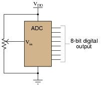
As the input voltage changes, the binary number output by the ADC will change as well. Suppose, though, that we want to have sample-and-hold capability added to this data acquisition circuit, to allow us to “freeze” the output of the ADC at will. Explain how using eight D latch circuits will give us this capability:
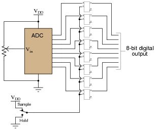
Reveal answerWhen the Sample/Hold switch is in the “low” position, the D latches all fall into the “latch” state, holding that last valid input states on their Q outputs.
Notes:Sample-and-hold circuitry is quite common in modern data acquisition and other types of electronic systems. In this case, sample-and-hold showcases a practical use of D latch circuits. If your students have not yet heard of analog-to-digital converters, it might be a good idea to discuss some of their general principles. No knowledge of their internal workings is necessary in order to comprehend the circuit shown in the question, however.
-
Question 18 of 26
Gated latch circuits often come packaged in multiple quantities, with common gate inputs, so that more than one of the latches within the integrated circuit will be enabled and disabled simultaneously. Examine this logic symbol, representative of the 74AC16373, a 16-bit D-type latch with tri-state outputs:

Note how the sixteen D latches are divided into two groups of eight. Explain the functions of the four inputs at the very top of the symbol (1EN, C1, 2EN, and C2). Which of these input lines correspond to the “Enable” inputs seen on single D-type latch circuits? Also, describe what the “wedge” shapes represent on the 1EN and 2EN input lines.
Suppose you wished to have all sixteen latch circuits enabled as one, rather than as two groups of eight. Show what you would have to do to this circuit in order to achieve this goal.
Reveal answerInputs C1 and C2 perform the standard “Enabling” function for the D-type latches within this integrated circuit. The 1EN and 2EN inputs control the tri-state outputs. Their “wedge” symbols mean “complemented,” and are equivalent to the “bubbles” seen on traditional gate symbols.
To make all sixteen latches enable and disable as one, bridge the enable inputs as such:

Notes:This question not only introduces students to the concept of multiple latches in a single integrated circuit, but it also shows an example of IEEE/ANSI “block” symbolism. Your students, having become well adjusted to the idea of independent research by now, should have obtained the datasheet for this circuit (74AC16373) as part of their study. The information contained in the datasheet should prove to be quite informative in answering their questions about enable input functions, tri-state outputs, and the like. If they haven’t obtained datasheets, and cannot understand the answers to the question(s), don’t just tell them - have them look it up for themselves!