Facebook
 Google
 GitHub
 Linkedin
Digital Circuits
CMOS Logic Gates
27 questions By Tony R. Kuphaldt
-
Question 4 of 27
The simplest type of digital logic circuit is an inverter, also called an inverting buffer, or NOT gate. Here is a schematic diagram for an inverter gate constructed from complementary MOSFETs (CMOS), shown connected to a SPDT switch and an LED:
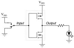
Determine the status of the LED in each of the input switch’s two positions. Denote the logic level of switch and LED in the form of a truth table:

Reveal answer
Notes:Have your students explain the operation of this very simple MOSFET circuit, describing how the inverse logic state is generated at the output terminal, from a given input state. Discuss with your students the simplicity of the CMOS inverter, especially contrasted against a TTL inverter circuit.
-
Question 5 of 27
Practical CMOS logic gates contain more than just MOSFETs. Here is a schematic diagram for a typical inverter gate circuit, with protection diodes:
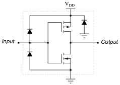
Explain what specific conditions each protection diode protects against.
Reveal answerTwo of the diodes protect against input voltages exceeding the supply rails, while the third diode protects against a reverse-connected power supply.
Notes:It is important that students realize these “protection” diodes do not allow circuit designers and builders to disregard good design practices with impunity. Ask your students, in each case, how each protection diode accomplishes its task of protecting the MOSFETs from damage. Does this mean the gate circuit will be able to withstand abnormal conditions indefinitely? Why or why not?
-
Question 6 of 27
A student builds the following digital circuit on a solderless breadboard (a “proto-board”):
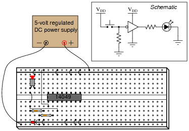
The DIP circuit is a hex inverter (it contains six “inverter” or “NOT” logic gates), but only one of these gates is being used in this circuit. The student’s intent was to build a logic circuit that energized the LED when the pushbutton switch was unactuated, and de-energized the LED when the switch was pressed: so that the LED indicates the reverse state of the switch itself. The student builds this circuit, and it is found to function perfectly well.
Explain the purpose of the resistor on the input of the inverter. What is it there for? What might happen if it were to be removed from the circuit?
Also, explain why the inputs of all the unused inverter gates in this IC have been either connected to ground or to VDD. Is this necessary for the circuit to work properly, or is it just a precautionary measure?
Reveal answerThe resistor on the input side of the gate functions as a pulldown, to provide a solid “low” state to the gate’s input when the switch contacts open.
Shorting all unused gate inputs to either ground or VDD is merely a precautionary measure. It prevents unnecessary power draw from the supply, and possible IC overheating.
Notes:Discuss the problem of “floating” or “high-Z” states with your students, especially in the context of CMOS. What is it about the nature of a CMOS circuit that makes floating inputs especially troublesome? Ask your students to contrast this against floating TTL inputs.