Facebook
 Google
 GitHub
 Linkedin
Digital Circuits
CMOS Logic Gates
27 questions By Tony R. Kuphaldt
-
Question 22 of 27
A very important concept to understand in digital circuitry is the difference between current sourcing and current sinking. For instance, examine this CMOS inverting buffer gate circuit, connected to a load:
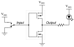
Is this gate circuit configured to source load current, sink load current, or do both?
Reveal answerIn this particular case, the way the load (LED) is connected to the output of the gate, the gate will only sink current. However, the gate is capable of sourcing current to a load, if only the load were connected differently.
Follow-up question: re-draw the circuit to show the gate sourcing current to an LED load.
Notes:This very important concept is best understood from the perspective of conventional current flow notation. The terms seem backward when electron flow notation is used to track current through the output transistor.
One point of confusion I’ve experienced among students is that current may go either direction (in or out) of a gate with totem-pole output transistors (able to sink or source current). Some students seem to have a conceptual difficulty with current going in to the output terminal of a gate circuit, because they mistakenly associate the “out” in output as being a reference to direction of current, rather than direction of information or data.
An analogy I’ve used to help students overcome this problem is that of two people carrying a long pole:
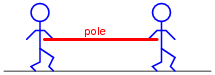
Suppose these people are in a dark, noisy room, and they use the pole as a means of simple communication between them. For example, one person could tug on the pole to get the other person’s attention. Perhaps they could even develop a simple code system for communicating thoughts (1 tug = hello ; 2 tugs = good-bye ; 3 tugs = I think this is a silly way to communicate ; 4 tugs = let’s leave this room ; etc.). If one of the persons pushes on the pole rather than pulls on the pole to get the other person’s attention, does the direction of the pole’s motion change the direction of the communication between the two persons? Of course not. Well, then, does the direction of current through the output terminal of a gate change the direction that information flows between two interconnected gates? Whether a gate sources current or sinks current to a load has no bearing on the “output” designation of that gate terminal. Either way, the gate is still “telling the load what to do” by exercising control over the load current.
-
Question 23 of 27
Suppose that a CMOS inverting buffer gate were to drive a predominantly inductive load, such as a small relay coil:
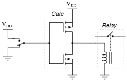
Normally, it would be considered good design practice to connect a commutating diode in parallel with the relay coil, to prevent high-voltage transients when the coil is de-energized. However, this is not necessary when a CMOS gate drives a coil. Explain why.
Reveal answerIf you thought the answer to this question was, “because MOSFET transistors are immune to damage from high-voltage transients,” you were wrong. If anything, MOSFETs are even more susceptible to damage from high-voltage transients than BJTs, given their thinly insulated gates.
The correct answer has to do with the bilateral (non polarity-sensitive) nature of MOSFETs when conducting. Trace the direction of current through the relay coil while energized, and at the point in time when the gate output switches to a “low” state, and you will understand why no commutating diode is necessary in this circuit.
Notes:By examining one of the ancillary benefits of using CMOS instead of TTL, students get a good review of inductor and transistor theory. Ask your students to explain why a TTL gate would require the relay coil to have a commutating diode, lest the gate be destroyed by inductive “kickback.”
-
Question 24 of 27
A problem unique to certain types of CMOS logic gates is something called SCR latchup. This is an abnormal condition capable of ruining a circuit, or at the very least causing operational problems in a circuit. Explain what this phenomenon is, and what causes it.
Reveal answerIf an input or output of a CMOS gate circuit is driven above VDD, even momentarily, the circuit may “latch” like an SCR, causing VDD to become shorted to VSS internally. This is made possible by the way CMOS transistors are manufactured on the integrated circuit’s substrate.
Challenge question: referencing a cross-sectional illustration of a CMOS gate integrated circuit, show the “SCR” formed by the transistors, and explain how it may be “fired” by excessive input voltage to the gate.
Notes:Based on their knowledge of thyristors, your students should be able to tell you how to best “unlatch” a CMOS gate stuck in this condition. Challenge them with this problem, and also with the question of how one might detect such a condition as it’s happening.
Mention to your students that not all CMOS families exhibit this problem, and that manufacturers have been keen to address serious design faults such as these. If nothing else, though, this should reinforce the lesson that one should never exceed the supply rail voltage for any type of active circuit, be it an op-amp, gate, or something else, unless expressly permitted by the manufacturer.