Facebook
 Google
 GitHub
 Linkedin
Digital Circuits
CMOS Logic Gates
27 questions By Tony R. Kuphaldt
-
Question 19 of 27
A student builds the following circuit to demonstrate the behavior of a NAND gate:
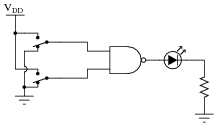
When the student tests the circuit, though, something is wrong:
- Both switches LOW, no light.
- One switch HIGH, the other switch LOW; LED lights up.
- One switch LOW, the other switch HIGH; LED lights up.
- Both switches HIGH, no light.
Instead of acting as a NAND gate should, it seems to behave as if it were an Exclusive-OR gate! Examining the circuit for mistakes, the student discovers missing power connections to the chip - in other words, neither VDD nor VSS are connected to the power source.
While this certainly is a problem, the student is left to wonder, “How did the circuit ever function at all?” With no power connected to the chip, how is it possible that the LED ever lit in any condition?
Reveal answerThe chip’s internal input protection diodes allowed the switch inputs to supply operating power to the MOSFET transistors.
Notes:As an instructor of electronics, I’ve seen students make this mistake countless times. What is particularly troublesome about this error is the seemingly intermittent behavior of the chip. Without power supplied to the chip, most students assume there would be no function at all. So when they see the chip functioning adequately in some of its circuit’s states, they are inclined to assume power is not an issue!
-
Question 20 of 27
What does it mean if you see a logic gate symbol in a schematic diagram with a strange-looking “S” figure drawn inside of it?

Reveal answerThe “S” figure, which resembles a magnetic B-H hysteresis curve, marks this gate as a Schmitt trigger. I’ll let you do the research to determine what this means in regard to gate function.
Notes:Schmitt trigger gates are indispensable for certain logic circuit applications. It is important that students recognize their function and utility.
Incidentally, this question provides a good opportunity to review magnetic hysteresis curves, since it’s probably been awhile since students last studied electromagnetism theory!
-
Question 21 of 27
In CMOS circuitry, one side of the DC power supply is usually labeled as “VDD”, while the other side is labeled as “VSS”. Why is this? What do the subscripts “DD” and “SS” represent?
Reveal answerThe labels VDD and VSS are supposed to mean “power supply to drain and source sides of MOSFETs, respectively. This nomenclature is actually a holdover from obsolete NMOS gate designs, which used N-channel MOSFETS exclusively. Even though it doesn’t make much sense in CMOS circuits (you’ll see why if you examine the internal schematic diagram for a CMOS gate), it is the standard way of denoting power supply terminals for CMOS circuits.
Follow-up question: what polarities do these respective labels represent?
Notes:Ahhh, the vestiges of yesterday’s technology! What can I say? Sometimes terms “stick” even when it makes little sense for them to.