Facebook
 Google
 GitHub
 Linkedin
Digital Circuits
CMOS Logic Gates
27 questions By Tony R. Kuphaldt
-
Question 16 of 27
A trend in CMOS logic gate development is toward lower and lower operating voltages. The “AUC” family of CMOS logic, for example, is able to operate at less than 2 volts VDD!
Explain why this is a trend in modern logic circuit design. What benefits result from lower operating voltages? What possible disadvantages also result?
Reveal answerLower operating voltages result in less power dissipation. However, noise margins become “tighter” under the same conditions, which is a disadvantage.
Notes:Discuss this trend with your students, citing examples from industry literature if possible. Be sure to ask your students why lower operating voltages reduces power dissipation (with reference to Joule’s Law, please!), and also why this reduces noise margins.
-
Question 17 of 27
Predict how the operation of this logic gate circuit will be affected as a result of the following faults. Consider each fault independently (i.e. one at a time, no multiple faults):
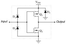
- Diode D1 fails open:
- Diode D1 fails shorted:
- Diode D2 fails open:
- Diode D2 fails shorted:
- Transistor Q1 fails open (drain to source):
- Transistor Q2 fails open (drain to source):
For each of these conditions, explain why the resulting effects will occur.
Reveal answer- Diode D1 fails open: No effect.
- Diode D1 fails shorted: Output always in low state, possible damage to circuit when input is forced low by another gate (or switch).
- Diode D2 fails open: No effect.
- Diode D2 fails shorted: Output always in high state, possible damage to circuit when input is forced high by another gate (or switch).
- Transistor Q1 fails open (drain to source): Output cannot source current in high state, but is still able to sink current in low state.
- Transistor Q2 fails open (drain to source): Output cannot sink current in low state, but is still able to source current in high state.
Notes:The purpose of this question is to approach the domain of circuit troubleshooting from a perspective of knowing what the fault is, rather than only knowing what the symptoms are. Although this is not necessarily a realistic perspective, it helps students build the foundational knowledge necessary to diagnose a faulted circuit from empirical data. Questions such as this should be followed (eventually) by other questions asking students to identify likely faults based on measurements.
-
Question 18 of 27
Identify at least three different transistor faults in this CMOS logic gate that could cause the output to fail low:
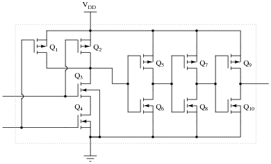
Reveal answer- Transistor Q1 failed shorted (drain to source).
- Transistor Q4 failed open (drain to source).
- Transistor Q5 failed open (drain to source).
- Transistor Q10 failed shorted (drain to source).
Notes:One way for students to approach this problem is to re-draw the schematic in gate symbol form, a NAND gate followed by three inverters:

Discuss with them why this approach may be helpful in determining possible component faults in the integrated circuit.