Facebook
 Google
 GitHub
 Linkedin
Digital Circuits
CMOS Logic Gates
27 questions By Tony R. Kuphaldt
-
Question 7 of 27
The following is an internal schematic of a CMOS logic gate. Based on your analysis of the transistor circuit, determine what type of gate (AND, OR, NAND, NOR, XOR, etc.) it is:

Reveal answerThis is a NOR gate.
Follow-up question: identify a series of “thought experiments” you could perform on this circuit schematic to determine the identity of the gate. In other words, document what imagined conditions you would subject this gate to, and what the resulting output states would signify, in answering the question of what type of gate this is.
Notes:CMOS logic gate circuits are the easiest of all the gates to analyze internally! Discuss with your students why the second-from-the-top MOSFET uses an independent substrate connection (as opposed to making it common with the source, as usual).
-
Question 8 of 27
What is the typical power supply voltage range for a CD4xxx series (or MC4xxx series) CMOS logic gate? How does this compare with the allowable power supply voltage range for a standard (5 volt) TTL logic gate? Consult a datasheet for your answer.
Reveal answer3 to 18 VDC is typical, though some integrated circuits may have slightly different ratings.
Notes:This question gets students in the habit of consulting datasheets to obtain information on logic gate circuits. Datasheets are a wealth of technical information, and students absolutely have to become adept at referencing them to obtain the information they need to build and troubleshoot logic circuits.
-
Question 9 of 27
A logic probe is a very useful tool for working with digital logic circuits. It indicates “high” and “low” logic states by means of LED’s, giving visual indication only if the voltage levels are appropriate for each state.
Here is a schematic diagram for a logic probe built using comparators. Each comparator has a threshold adjustment potentiometer, so that it may be set to indicate its respective logic state only if the signal voltage is well within the range stated by the logic manufacturer:
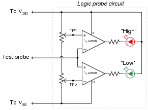
When this logic probe circuit is connected to the VDD and VSS power supply terminals of a powered CMOS circuit, what voltage levels should test points TP1 and TP2 be adjusted to, in order for the probe to properly indicate “high” and “low” CMOS logic states? Consult a datasheet for the quad NAND gate numbered 4011. This is a legacy CMOS integrated circuit.
Reveal answerI’ll let you do your own research on this question. DO NOT obtain your answer from a textbook, but consult a manufacturer’s datasheet instead! You will find that the acceptable voltage levels vary with the power supply voltage, but that the percentages are rather constant.
Follow-up question: write a formula for calculating appropriate current-limiting resistor sizes for the two LEDs in this circuit, given the value of V and the LED forward voltage and current values.
Challenge question: the logic probe circuit shown is minimal in component count. To make a more practical and reliable probe, one would probably want to have reverse-polarity protection (in case someone were to accidentally connect the probe backward across the power supply) as well as decoupling for immunity against electrical noise. Add whatever necessary components you think there should be in this circuit to provide these features.
Notes:The most obvious lesson of this question is to introduce (or review as the case may be) the purpose and operation of a logic probe. However, this question is also a veiled introduction (or review) of CMOS logic levels.