Facebook
 Google
 GitHub
 Linkedin
Discrete Semiconductor Devices and Circuits
Junction field-effect transistors (JFET)
43 questions By Tony R. Kuphaldt
-
Question 4 of 43
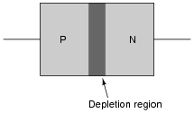
The dark shaded area drawn in this cross-section of a PN junction represents the depletion region:
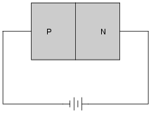
Re-draw the depletion region when the PN junction is subjected to a reverse-bias voltage:
Reveal answer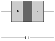
Follow-up questions: describe the conductivity of the depletion region: is it high or low? What exactly does the word “depletion” refer to, anyway?
Notes:This question makes a good lead-in to a discussion of JFET operation, where the channel conductivity is modulated by the width of the gate-channel depletion region.
-
Question 5 of 43
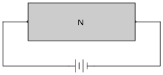
A field-effect transistor is made from a continuous “channel” of doped semiconductor material, either N or P type. In the illustration shown below, the channel is N-type:

Trace the direction of current through the channel if a voltage is applied across the length as shown in the next illustration. Determine what type of charge carriers (electrons or holes) constitute the majority of the channel current:
The next step in the fabrication of a field-effect transistor is to implant regions of oppositely-doped semiconductor on either side of the channel as shown in the next illustration. These two regions are connected together by wire, and called the “gate” of the transistor:
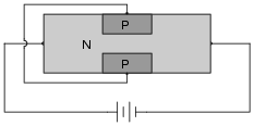
Show how the presence of these “gate” regions in the channel influence the flow of charge carriers. Use small arrows if necessary to show how the charge carriers move through the channel and past the gate regions of the transistor. Finally, label which terminal of the transistor is the source and which terminal is the drain, based on the type of majority charge carrier present in the channel and the direction of those charge carriers’ motion.
Reveal answerThe majority charge carriers in this transistor’s channel are electrons, not holes. Thus, the arrows drawn in the following diagrams point in the direction of electron flow:

This makes the right-hand terminal the source and the left-hand terminal the drain.
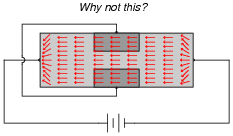
Follow-up question: explain why the charge carriers avoid traversing the PN junctions formed by the gate-channel interfaces. In other words, explain why we do not see this happening:
Notes:Students typically find junction field-effect transistors much easier to understand than bipolar junction transistors, because there is less understanding of energy levels required to grasp the operation of JFETs than what is required to comprehend the operation of BJTs. Still, students need to understand how different charge carriers move through N- and P-type semiconductors, and what the significance of a depletion region is.
-
Question 6 of 43
Field-effect transistors (FETs) exhibit depletion regions between the oppositely-doped gate and channel sections, just as diodes have depletion regions between the P and N semiconductor halves. In this illustration, the depletion region appears as a dark, shaded area:
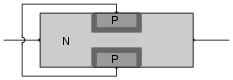
Re-draw the depletion regions for the following scenarios, where an external voltage (VGS) is applied between the gate and channel:
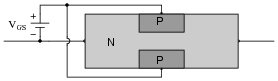

Note how the different depletion region sizes affect the conductivity of the transistor’s channel.
Reveal answer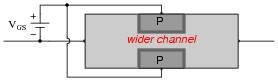
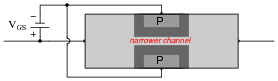
Follow-up question: why do you suppose this type of transistor is called a field-effect transistor? What “field” is being referred to in the operation of this device?
Notes:The effect that this external gate voltage has on the effective width of the channel should be obvious, leading students to understand how a JFET allows one signal to exert control over another (the basic principle of any transistor, field-effect or bipolar).