Facebook
 Google
 GitHub
 Linkedin
Digital Circuits
TTL Logic Gates
25 questions By Tony R. Kuphaldt
-
Question 7 of 25
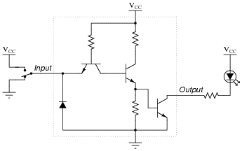
A very important concept to understand in digital circuitry is the difference between current sourcing and current sinking. For instance, examine this open-collector TTL inverter gate circuit, connected to a load:
Open-collector gates are specially designated in their schematic symbols by a marker within the gate shape:

Is this gate circuit able to source load current, sink load current, or do both?
Reveal answerOpen-collector gate circuits are only able to sink load current. They cannot “source” any load current at all.
Follow-up question #1: what would need to be added to the gate circuit shown, in order for it to have the ability to source load current as well as sink load current?
Follow-up question #2: explain how you would calculate current sinking ability of this logic gate circuit, if you were given the internal component values and parameters.
Notes:The very important concept of sourcing versus sinking is best understood from the perspective of conventional current flow notation. The terms seem backward when electron flow notation is used to track current through the output transistor.
One point of confusion I’ve experienced among students is that current may go either direction (in or out) of a gate with totem-pole output transistors (able to sink or source current). Some students seem to have a conceptual difficulty with current going in to the output terminal of a gate circuit, because they mistakenly associate the “out” in output as being a reference to direction of current, rather than direction of information or data.
An analogy I’ve used to help students overcome this problem is that of two people carrying a long pole:

Suppose these people are in a dark, noisy room, and they use the pole as a means of simple communication between them. For example, one person could tug on the pole to get the other person’s attention. Perhaps they could even develop a simple code system for communicating thoughts (1 tug = hello ; 2 tugs = good-bye ; 3 tugs = I think this is a silly way to communicate ; 4 tugs = let’s leave this room ; etc.). If one of the persons pushes on the pole rather than pulls on the pole to get the other person’s attention, does the direction of the pole’s motion change the direction of the communication between the two persons? Of course not. Well, then, does the direction of current through the output terminal of a gate change the direction that information flows between two interconnected gates? Whether a gate sources current or sinks current to a load has no bearing on the “output” designation of that gate terminal. Either way, the gate is still “telling the load what to do” by exercising control over the load current.
Ask your students to explain what the term “open-collector” means with reference to a TTL logic gate. How does this type of gate compare with normal (“totem pole” output) TTL gates?
-
Question 8 of 25
Based on an analysis of a typical TTL logic gate circuit (consult a datasheet for a TTL logic gate if you need an internal schematic diagram for a gate circuit), determine what logic state is “assumed” by a TTL gate input when left “floating” (disconnected).
What ramification does this have for us when choosing input devices for TTL logic gates? If, for instance, we wished to use a single-pole, single-throw (SPST) switch as the input device for a TTL logic gate, what is the best way to connect such a device to a TTL input? Should the switch connect the TTL input to VCC when closed, or should it connect the input to VEE when closed? Why does it matter? Explain your answer in detail.
Reveal answerTTL input devices must be current-sinking: that is, they must ground the TTL gate input in one of their states. I’ll let you figure out why this is so, from the schematic diagrams of TTL logic gate circuits.
Notes:For review, ask your students what the symbols VCC and VEE mean with reference to TTL circuits.
Proper TTL “etiquette” is vitally important for students to understand, if they are to successfully build digital circuits (especially when interfacing TTL with other types of logic!).
-
Question 9 of 25
A logic probe is a very useful tool for working with digital logic circuits. It indicates “high” and “low” logic states by means of LED’s, giving visual indication only if the voltage levels are appropriate for each state.
Here is a schematic diagram for a logic probe built using comparators. Each comparator has a threshold adjustment potentiometer, so that it may be set to indicate its respective logic state only if the signal voltage is well within the range stated by the logic manufacturer:
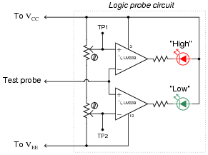
When this logic probe circuit is connected to the VCC and VEE power supply terminals of a powered TTL circuit, what voltage levels should test points TP1 and TP2 be adjusted to, in order for the probe to properly indicate “high” and “low” TTL logic states? Consult a datasheet for the quad NAND gate numbered either 74LS00 or 54LS00. Both are legacy TTL integrated circuits.
Reveal answerI’ll let you do your own research on this question. DO NOT obtain your answer from a textbook, but consult a manufacturer’s datasheet instead!
Follow-up question: given the standard VCC voltage level of 5.0 volts for TTL circuits, and assuming the use of LEDs that drop 1.7 volts at 20 mA, calculate an appropriate resistance value for the two LED current-limiting resistors.
Challenge question: the logic probe circuit shown is minimal in component count. To make a more practical and reliable probe, one would probably want to have reverse-polarity protection (in case someone were to accidentally connect the probe backward across the power supply) as well as decoupling for immunity against electrical noise. Add whatever necessary components you think there should be in this circuit to provide these features.
Notes:The most obvious lesson of this question is to introduce (or review as the case may be) the purpose and operation of a logic probe. However, this question is also a veiled introduction (or review) of TTL logic levels.