Facebook
 Google
 GitHub
 Linkedin
Discrete Semiconductor Devices and Circuits
Power Conversion Circuits
30 questions By Tony R. Kuphaldt
-
Question 7 of 30
The schematic diagram shown here is for a “boost” converter circuit, a type of DC-DC “switching” power conversion circuit:
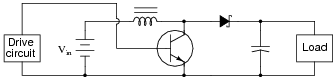
In this circuit, the transistor is either fully on or fully off; that is, driven between the extremes of saturation or cutoff. By avoiding the transistor’s “active” mode (where it would drop substantial voltage while conducting current), very low transistor power dissipations can be achieved. With little power wasted in the form of heat, “switching” power conversion circuits are typically very efficient.
Trace all current directions during both states of the transistor. Also, mark the inductor’s voltage polarity during both states of the transistor.
Reveal answer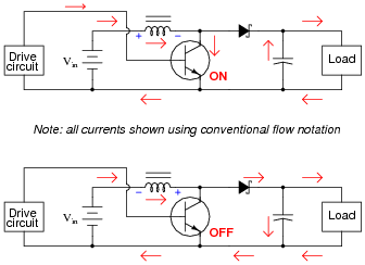
Follow-up question: how does the load voltage of this converter relate to the supply (battery) voltage? Does the load receive more or less voltage than that provided by the battery?
Challenge question: why do you suppose a Schottky diode is used in this circuit, as opposed to a regular (PN) rectifying diode?
Notes:Ask your students why they think this circuit is called a boost converter. “Boost” usually refers to something that is aiding something else. What is being aided in this circuit?
-
Question 8 of 30
The schematic diagram shown here is for an “inverting” converter circuit, a type of DC-DC “switching” power conversion circuit:
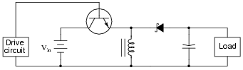
In this circuit, the transistor is either fully on or fully off; that is, driven between the extremes of saturation or cutoff. By avoiding the transistor’s “active” mode (where it would drop substantial voltage while conducting current), very low transistor power dissipations can be achieved. With little power wasted in the form of heat, switching” power conversion circuits are typically very efficient.
Trace all current directions during both states of the transistor. Also, mark the inductor’s voltage polarity during both states of the transistor.
Reveal answer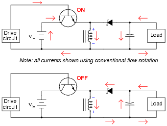
Notes:Ask your students why they think this circuit is called an inverting converter.
Although it may not be evident from viewing the circuit schematic, this converter circuit is capable of stepping voltage up or down, making it quite versatile.
-
Question 9 of 30
The schematic diagram shown here is for a “Cuk” converter circuit, a type of DC-DC “switching” power conversion circuit:
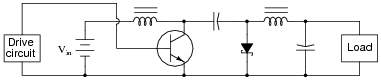
In this circuit, the transistor is either fully on or fully off; that is, driven between the extremes of saturation or cutoff. By avoiding the transistor’s “active” mode (where it would drop substantial voltage while conducting current), very low transistor power dissipations can be achieved. With little power wasted in the form of heat, “switching” power conversion circuits are typically very efficient.
Trace all current directions during both states of the transistor. Also, mark the both inductors’ voltage polarities during both states of the transistor.
Reveal answer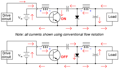
Follow-up question: how does the load voltage of this converter relate to the supply (battery) voltage? Does the load receive more or less voltage than that provided by the battery?
Notes:The “strange” name of this circuit comes from the last name of the engineer who invented it! For more information, consult the writings of Rudy Severns on the general topic of switch-mode power conversion circuits.