Facebook
 Google
 GitHub
 Linkedin
Discrete Semiconductor Devices and Circuits
Performance-Based Assessments for Semiconductor Circuit Competencies
62 questions By Tony R. Kuphaldt
-
Question 52 of 62
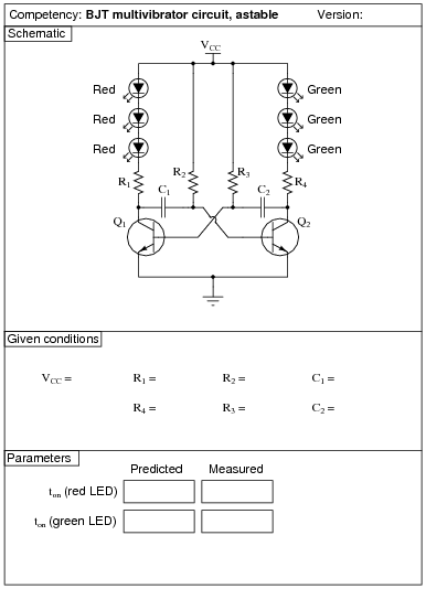
Reveal answerUse circuit simulation software to verify your predicted and measured parameter values.
Notes:Use a variable-voltage, regulated power supply to supply any amount of DC voltage below 30 volts. Specify standard resistor values, all between 1 kΩ and 100 kΩ (1k5, 2k2, 2k7, 3k3, 4k7, 5k1, 6k8, 10k, 22k, 33k, 39k 47k, 68k, etc.).
This circuit produces nice, sharp-edged square wave signals at the transistor collector terminals when resistors R1 and R4 are substantially smaller than resistors R2 and R3. This way, R2 and R3 dominate the capacitors’ charging times, making calculation of duty cycle much more accurate. Component values I’ve used with success are 470 Ω for R1 and R2, 270 kΩ for R2 and R3, 4.7 μF for C1 and C2, and 6 to 14 volts for VCC. The frequency of this circuit does vary with supply voltage, so don’t expect perfect agreement between predicted and measured values.
By the way, this circuit works very well for holiday flashing lights - decorate your lab room accordingly with student-built light flashers!
An extension of this exercise is to incorporate troubleshooting questions. Whether using this exercise as a performance assessment or simply as a concept-building lab, you might want to follow up your students’ results by asking them to predict the consequences of certain circuit faults.
-
Question 53 of 62
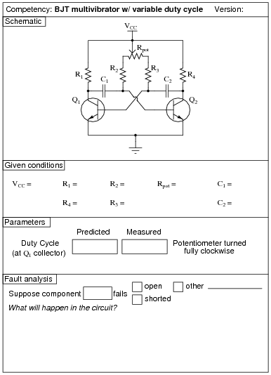
Reveal answerUse circuit simulation software to verify your predicted and measured parameter values.
Notes:Use a variable-voltage, regulated power supply to supply any amount of DC voltage below 30 volts. Specify standard resistor values, all between 1 kΩ and 100 kΩ (1k5, 2k2, 2k7, 3k3, 4k7, 5k1, 6k8, 10k, 22k, 33k, 39k 47k, 68k, etc.).
This circuit produces nice, sharp-edged square wave signals at the transistor collector terminals when resistors R1 and R4 are substantially smaller than the combined resistance of resistors R2 and R3 and the respective potentiometer section resistances. This way, Rpot, R2, and R3 dominate the capacitors’ charging times, making calculation of duty cycle much more accurate. Component values I’ve used with success are 1 kΩ for R1 and R2, 10 kΩ for R2 and R3, 100 kΩ for Rpot, and 0.001 μF for C1 and C2.
An extension of this exercise is to incorporate troubleshooting questions. Whether using this exercise as a performance assessment or simply as a concept-building lab, you might want to follow up your students’ results by asking them to predict the consequences of certain circuit faults.
-
Question 54 of 62
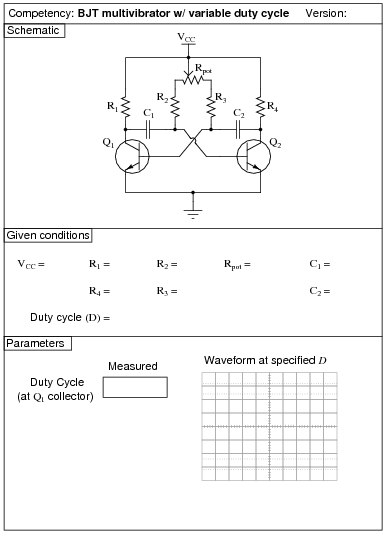
Reveal answerUse circuit simulation software to verify your predicted and measured parameter values.
Notes:Use a variable-voltage, regulated power supply to supply any amount of DC voltage below 30 volts. Specify standard resistor values, all between 1 kΩ and 100 kΩ (1k5, 2k2, 2k7, 3k3, 4k7, 5k1, 6k8, 10k, 22k, 33k, 39k 47k, 68k, etc.).
This circuit produces nice, sharp-edged square wave signals at the transistor collector terminals when resistors R1 and R4 are substantially smaller than the combined resistance of resistors R2 and R3 and the respective potentiometer section resistances. This way, Rpot, R2, and R3 dominate the capacitors’ charging times, making calculation of duty cycle much more accurate. Component values I’ve used with success are 1 kΩ for R1 and R2, 10 kΩ for R2 and R3, 100 kΩ for Rpot, and 0.001 μF for C1 and C2.
An extension of this exercise is to incorporate troubleshooting questions. Whether using this exercise as a performance assessment or simply as a concept-building lab, you might want to follow up your students’ results by asking them to predict the consequences of certain circuit faults.