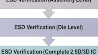
Take a look at verification challenges and walk through a proven automated ESD verification methodology for 2.5D and 3D ICs.
Take a look at verification challenges and walk through a proven automated ESD verification methodology for 2.5D and 3D ICs.

Learn how to quickly and accurately analyze and fix (or waive) a wide range of complex error conditions with automated…
Learn how to quickly and accurately analyze and fix (or waive) a wide range of complex error conditions with automated post-processing DRC debugging flows.

This paper outlines the multi-dimensional nature of this complexity and the costs and opportunities it generates. It also…
This paper outlines the multi-dimensional nature of this complexity and the costs and opportunities it generates. It also demonstrates that the key to designers meeting this challenge is the ability to attain system-level visibility: both during the semiconductor development cycle, and subsequently after embedded systems are deployed in the field.

This white paper describes Siemens' new cloud-based solution and provides use-case examples. Readers will also get a…
This white paper describes Siemens' new cloud-based solution and provides use-case examples. Readers will also get a detailed description and testimonial from an early adopter.

This white paper displays how the Tanner flow simplifies the design and verification process of Analog/Mixed-Signal…
This white paper displays how the Tanner flow simplifies the design and verification process of Analog/Mixed-Signal design. It also describes how the user can verify design functionality, connectivity, and performance at all levels of the design hierarchy and for all integrated circuit (IC) applications.

This white paper walks through the design and review of a wiring harness for a small tractor using VeSys. Solutions like…
This white paper walks through the design and review of a wiring harness for a small tractor using VeSys. Solutions like the one discussed in this resource allow vehicle manufacturers to meet the demands of product complexity and quality while going to market faster than ever.

In this white paper, the reader will learn how the Calibre tools provide enhanced verification and fill optimization…
In this white paper, the reader will learn how the Calibre tools provide enhanced verification and fill optimization that can drastically reduce the number of simulations required. It also discusses how the tools achieve the aforementioned while still ensuring designs will perform reliably in conformance with their design specifications over the lifetime of the products in which they are used.

This white paper looks at the challenges of ever-increasingly complex designs packed into each die and explores…
This white paper looks at the challenges of ever-increasingly complex designs packed into each die and explores techniques that can be used to close designs efficiently and deliver them on time.

This white paper outlines how to simplify the analog management process by rolling all the tasks into a single tool that…
This white paper outlines how to simplify the analog management process by rolling all the tasks into a single tool that also enables the visualization of results in spreadsheets.

This paper shows how manufacturing requirements can be leveraged to perform automated insertion of DRC/LVS-clean vias.
This paper shows how manufacturing requirements can be leveraged to perform automated insertion of DRC/LVS-clean vias.
Among the challenges for design-for-test (DFT) engineers is how to set a target metric for automatic test pattern…
Among the challenges for design-for-test (DFT) engineers is how to set a target metric for automatic test pattern generation (ATPG) and how to choose the best set of patterns. Traditional coverage targets based on the number of faults detected don’t consider the likelihood of one fault occurring compared to another.

This white paper demonstrates how using a production 7nm design, AMD achieved a 2.5X speed up in physical verification cycle time.
This white paper demonstrates how using a production 7nm design, AMD achieved a 2.5X speed up in physical verification cycle time.

This white paper takes a look at how to replace inefficient, less precise verification processes with smarter, more…
This white paper takes a look at how to replace inefficient, less precise verification processes with smarter, more accurate, faster, and more efficient functionality that can improve both the bottom line and product quality.

This white paper evaluates the necessity and value of EDA in the cloud while providing a cost-benefit breakdown.…
This white paper evaluates the necessity and value of EDA in the cloud while providing a cost-benefit breakdown. Additionally, explore how companies can establish guidelines to ensure that usage is as efficient and cost-effective as possible.

This white paper takes a closer look at how cloud processing provides companies the opportunity to reduce time to market…
This white paper takes a closer look at how cloud processing provides companies the opportunity to reduce time to market and speed up innovation while maintaining or lowering operating costs. This resource also describes what makes Core Calibre technology cloud-ready and its improvements in cloud security that eliminate industry concern over IP protection.

This paper provides an overview of the key characteristics of ON Semiconductor Gen 1 1200 V SiC MOSFETs and how they can…
This paper provides an overview of the key characteristics of ON Semiconductor Gen 1 1200 V SiC MOSFETs and how they can be influenced by the driving conditions. This resource also provides a guideline on the usage of the NCP51705 an isolated gate driver for SiC MOSFETs.

Some engineers believe that the 2D design is no longer sufficient for today’s complicated PCB layouts. Flex and…
Some engineers believe that the 2D design is no longer sufficient for today’s complicated PCB layouts. Flex and rigid-flex designs, and an increasing need for collaboration with MCAD, require advanced 3D layout design capabilities to address today’s challenges fully.

A new metric for SerDes channel and package characterization is emerging. Effective Return Loss (ERL) is replacing the…
A new metric for SerDes channel and package characterization is emerging. Effective Return Loss (ERL) is replacing the traditional frequency-domain Return Loss (RL) metric as a more effective means of characterizing SerDes channels.

DDRx memory interfaces are key enablers for the technology that shapes modern life. Servers, computers, smartphones,…
DDRx memory interfaces are key enablers for the technology that shapes modern life. Servers, computers, smartphones, gaming consoles, and GPS systems are just some of the products that demand high-speed, high-bandwidth, double-data-rate memory. Each generation of DDRx DRAM brings new advantages that allow for faster, higher-capacity, and lower-power-consumption products.

Moving some or all of your electronic design automation (EDA) computing to the cloud enables your company to reduce…
Moving some or all of your electronic design automation (EDA) computing to the cloud enables your company to reduce time-to-market and innovate faster, simply by taking advantage of flexible resources and economies of scale.
 Facebook
 Google
 GitHub
 Linkedin