Designers must consider processing temperatures, producibility, and solder joint integrity of every component as well as higher I/O connectors. This article…
Designers must consider processing temperatures, producibility, and solder joint integrity of every component as well as higher I/O connectors. This article looks at ways to enable smaller component footprints for high-density PCBs.

This article discusses why verification and validation matter in design, how they differ, and how applications help teams…
This article discusses why verification and validation matter in design, how they differ, and how applications help teams incorporate and enrich their workflows.

The new PSPICE for TI enables engineers to simulate complex analog circuits with unlimited analysis of TI power and…
The new PSPICE for TI enables engineers to simulate complex analog circuits with unlimited analysis of TI power and signal-chain products.

MCAD and ECAD have inserted themselves into most design engineers' day-to-day work. Although familiar, both programs have…
MCAD and ECAD have inserted themselves into most design engineers' day-to-day work. Although familiar, both programs have come a long way and are continuing to evolve. In this article, learn the past and future of these design tools.

Getting an end-of-life notice on a component can be a major setback for both new and existing designs. How do you work…
Getting an end-of-life notice on a component can be a major setback for both new and existing designs. How do you work around the inconvenience?

A new project indicates the value of 3D printing in PCB design: fast prototyping.
A new project indicates the value of 3D printing in PCB design: fast prototyping.

The AI platform from the Fraunhofer Institute for Applied Information Technology (FIT) is comprised of modules for…
The AI platform from the Fraunhofer Institute for Applied Information Technology (FIT) is comprised of modules for artificial intelligence, machine learning, and deep learning.

This FEQ (Frequent Engineering Question) gives you essential information about the most important and widespread…
This FEQ (Frequent Engineering Question) gives you essential information about the most important and widespread technique for converting a theoretical circuit into a functional physical device.

Social distancing doesn't mean your productivity must come to a halt.
Social distancing doesn't mean your productivity must come to a halt.

MIT has developed a software design kit that speeds up electronic device development and prototyping by creating curved…
MIT has developed a software design kit that speeds up electronic device development and prototyping by creating curved breadboards with pinholes and connections mapped out automatically.

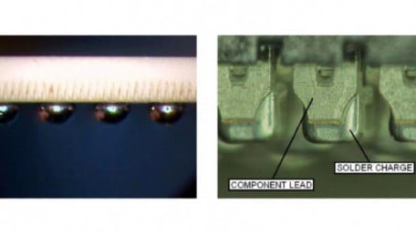
Pick-and-place can damage sensitive parts and contactless methods are inefficient for high volumes. What about magnetic assembly?
Pick-and-place can damage sensitive parts and contactless methods are inefficient for high volumes. What about magnetic assembly?

In this article, engineers discuss seemingly primitive parts of the manufacturing process and the feasibility of…
In this article, engineers discuss seemingly primitive parts of the manufacturing process and the feasibility of replacing those processes with automation.

inspectAR offers engineers a revolutionary new method of interacting with PCBs using the power of augmented reality.
inspectAR offers engineers a revolutionary new method of interacting with PCBs using the power of augmented reality.

This article looks at the common options for a four-layer board stackup.
This article looks at the common options for a four-layer board stackup.

This article discusses the major causes of high temperatures on PCBs that cause failure and damage to the board itself.
This article discusses the major causes of high temperatures on PCBs that cause failure and damage to the board itself.

TDK joins a list of companies who provide test-based models for RF and mmWave components through Modelithics.
TDK joins a list of companies who provide test-based models for RF and mmWave components through Modelithics.

Learn how to use the gridded ground technique to reduce noise in a double-sided PCB.
Learn how to use the gridded ground technique to reduce noise in a double-sided PCB.

The design of a modern IC is a truly monumental undertaking, and IC design tools make the job possible.
The design of a modern IC is a truly monumental undertaking, and IC design tools make the job possible.

Ever wish you could see your design file layers overtop your spun board? Augmented reality may make that possible in real time.
Ever wish you could see your design file layers overtop your spun board? Augmented reality may make that possible in real time.

Learn best layout practices for your DC-DC buck converter circuits.
Learn best layout practices for your DC-DC buck converter circuits.
 Facebook
 Google
 GitHub
 Linkedin