Sending static PDFs and Gerbers for feedback is killing your project timelines and leading to costly PCB rework. Learn how to break down engineering silos and…
Sending static PDFs and Gerbers for feedback is killing your project timelines and leading to costly PCB rework. Learn how to break down engineering silos and modernize your PCB design reviews.

Learn how SoC integration impacts SMT assembly yield, from fine-pitch BGA challenges and package warpage to reflow…
Learn how SoC integration impacts SMT assembly yield, from fine-pitch BGA challenges and package warpage to reflow profiling and inspection strategies.

HDLs are formal descriptions of behavior, making them software by definition. Modernizing these outdated tools is key to…
HDLs are formal descriptions of behavior, making them software by definition. Modernizing these outdated tools is key to making FPGA development more accessible and productive for all engineers.

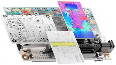
Modern SoC Evaluation Boards demand high-performance design, SI/PI, and system validation. Faraday offers 3 flexible…
Modern SoC Evaluation Boards demand high-performance design, SI/PI, and system validation. Faraday offers 3 flexible service levels to meet these complexities.

Learn how to prevent costly assembly delays by synchronizing ECAD and MCAD workflows through continuous 3D validation.…
Learn how to prevent costly assembly delays by synchronizing ECAD and MCAD workflows through continuous 3D validation. This also stabilizes production and eliminates mid-cycle re-spins.

Advanced packaging is at a crossroads due to AI demand. Learn the four emerging paths—CoWoS, CoPoS, glass-core, and…
Advanced packaging is at a crossroads due to AI demand. Learn the four emerging paths—CoWoS, CoPoS, glass-core, and CoWoP—and how to choose the right one for your multi-die system design.

The shift to 3D ICs and chiplets demands automated, hierarchical design planning to manage exploding pin counts. Learn…
The shift to 3D ICs and chiplets demands automated, hierarchical design planning to manage exploding pin counts. Learn how Siemens EDA's Innovator3D IC addresses these challenges.

This article explores how digital twins can help to reshape the design methodology of automotive semiconductors and…
This article explores how digital twins can help to reshape the design methodology of automotive semiconductors and systems, enabling truly software-defined vehicles.

FPGAs are limited by outdated proprietary software. Learn how embracing open-source tools is necessary to modernize FPGA…
FPGAs are limited by outdated proprietary software. Learn how embracing open-source tools is necessary to modernize FPGA development and unlock their full potential.

In today's rapidly evolving aerospace and defense landscape, component engineers face an unprecedented challenge:…
In today's rapidly evolving aerospace and defense landscape, component engineers face an unprecedented challenge: ensuring every part they specify meets stringent compliance requirements while maintaining mission readiness and program viability.

Memory selection has become a priority, as AI system designs demand more memory. Learn how to navigate hardware designs…
Memory selection has become a priority, as AI system designs demand more memory. Learn how to navigate hardware designs impacts and supply chain issues, and how BOM management tools help smooth the way.

Learn how PMIC.AI leverages custom LLM technology to transform how engineers design power supplies that meet the…
Learn how PMIC.AI leverages custom LLM technology to transform how engineers design power supplies that meet the increasing complexity of multi-rail SoC systems.

Learn how single-chip programmable logic devices (PLDs) can replace multiple discrete components used in power-up…
Learn how single-chip programmable logic devices (PLDs) can replace multiple discrete components used in power-up sequencing circuits to save cost and PCB area.

Learn how open source silicon can provide better security than traditional measures like obscurity, but only if employed…
Learn how open source silicon can provide better security than traditional measures like obscurity, but only if employed correctly, managed well, and backed with appropriate resources.

In PCB design, using grounded copper pour can be a double-edged sword. Learn how to make smart design decisions on…
In PCB design, using grounded copper pour can be a double-edged sword. Learn how to make smart design decisions on balancing copper layers, preventing dead copper issues, and enhancing PCB performance.

As data center computing and HPC advances, the stakes for ensuring reliability are high. Learn how to develop a silicon…
As data center computing and HPC advances, the stakes for ensuring reliability are high. Learn how to develop a silicon lifecycle management (SLM) strategy that ensures a successful future for your designs.

Rich resources are available today for crafting an enclosure using 3D printing. But where to begin? In this article,…
Rich resources are available today for crafting an enclosure using 3D printing. But where to begin? In this article, learn—step by step—how to design your own custom 3D printed electronics enclosure.

Improve your PCB designs and avoid costly respins due to EMC test failures by learning some basic design techniques and…
Improve your PCB designs and avoid costly respins due to EMC test failures by learning some basic design techniques and applying modern EMC analysis software.

Avoid mistakes when exporting PCB files from your EDA tools into the Gerber format by understanding the translation…
Avoid mistakes when exporting PCB files from your EDA tools into the Gerber format by understanding the translation process and using DFM tools.

Gerber layers don’t have to be a mystery. Knowing the names and purposes of each Gerber layer used in PCB manufacturing…
Gerber layers don’t have to be a mystery. Knowing the names and purposes of each Gerber layer used in PCB manufacturing can improve your designs and ease communication with the board house.
 Facebook
 Google
 GitHub
 Linkedin